
Lightwave Circuit and Method for Manufacturing Same

a technology of lightwave circuit and manufacturing method, which is applied in the direction of optical waveguide light guide, instruments, applications, etc., can solve the problems of increased light loss, reduced light loss, and reduced light loss, so as to reduce optical power loss and light loss and optical power split ratio of branch lightwave circuit, the effect of reducing optical power loss

Inactive Publication Date: 2014-01-23
LEE SEO YOUNG
View PDF12 Cites 39 Cited by
  • Summary
  • Abstract
  • Description
  • Claims
  • Application Information

AI Technical Summary

Benefits of technology

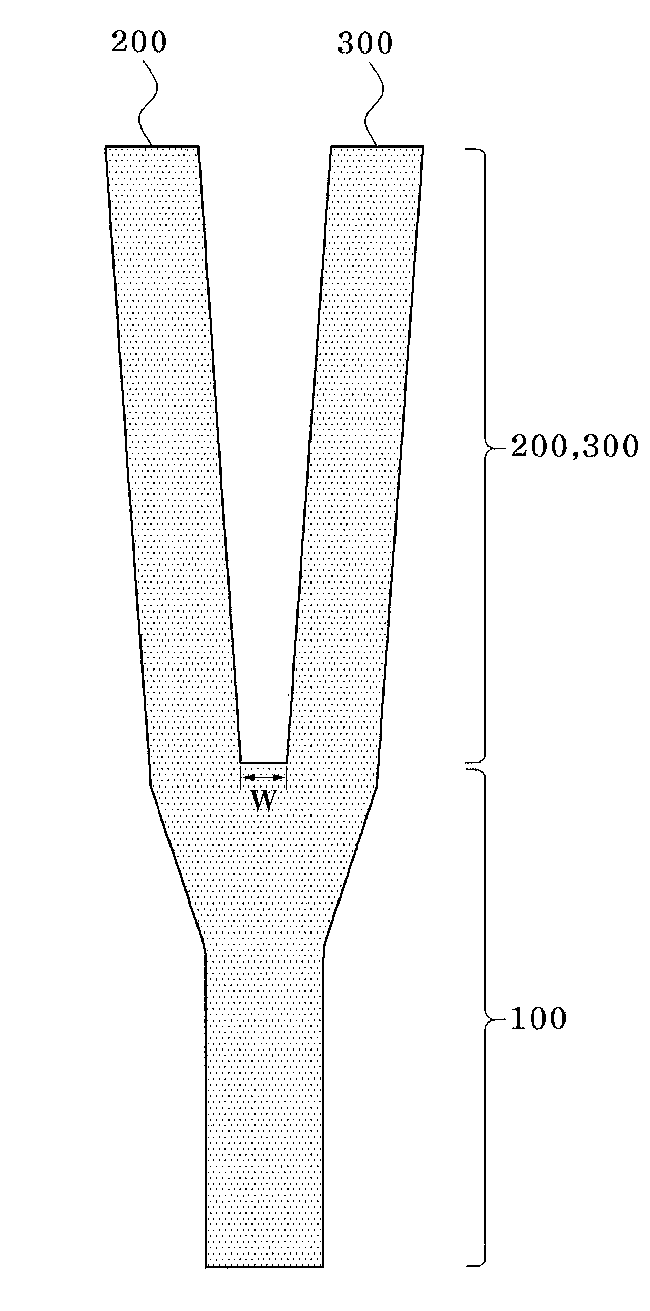
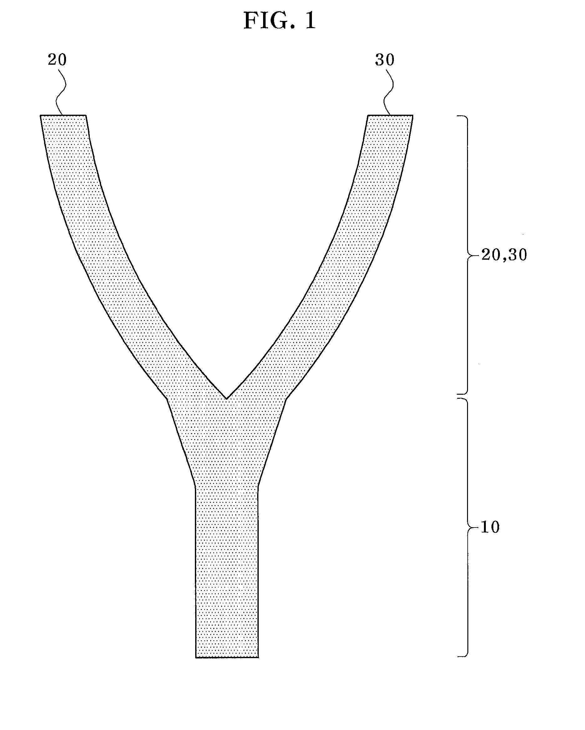
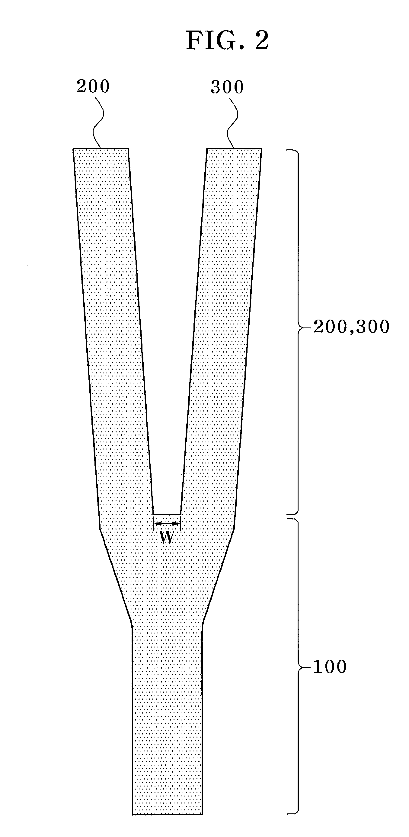
The present invention provides a method for improving the optical power split ratio and preventing damage at branches in a lightwave circuit. By using an engraved lightwave circuit core and a non-contact photo process, a high-quality lightwave circuit can be manufactured. Additionally, the invention allows for the use of larger wafers and increases productivity. The use of an engraved core process also reduces light loss and improves the interval between inner sides of output lightwave circuits compared to a Y-branch manufactured in an embossed core process.

Problems solved by technology

However, since the epoxy is largely different from the PLC in material characteristics, distortion or detachment may occur due to changes in temperature / humidity.
Further, when bonding the substrate of the PLC and the lid glass, considerable and additional manufacturing efforts such as thickness control of the epoxy with respect to the entire surface of the substrate are required.
Accordingly, in order to solve the problem, oxide additives such as boron oxide (B2O3), phosphorus pentoxide (P2O5) are heavily doped into the lid clad material, and then the core is melted and damaged by the lid clad in the lid clad process and the light loss is increased.
Further, the lid clad process is a process requiring a long time to deposit a very thick film with a thickness of about 20 to 40 microns.
Accordingly, productivity is greatly reduced, Further, the lightwave circuit core receives a stress due to a large difference in thermal expansion coefficients between two materials configuring a bottom clad substrate of a quartz glass and a heavily doped thick lid clad, and thus degradation of branching uniformity, particularly, polarization dependent loss (PDL), is increased.
Accordingly, no commercial apparatus is appropriate for this, much time and effort are needed to deposit the thick film as an optical film with high quality, and thus the lid clad process is the most difficult process in manufacturing PLCs.

Method used


Image

  • Lightwave Circuit and Method for Manufacturing Same
  • Lightwave Circuit and Method for Manufacturing Same
  • Lightwave Circuit and Method for Manufacturing Same

Examples


Embodiment Construction

[0050]Hereinafter, exemplary embodiments of the present invention will be described in detail. However, the present invention is not limited to the exemplary embodiments disclosed below, but can be implemented in various forms. The following exemplary embodiments are described in order to enable those of ordinary skill in the art to embody and practice the invention.

[0051]It will be understood that, although the terms first, second, etc. may be used herein to describe various elements, these elements should not be limited by these terms. These terms are only used to distinguish one element from another. For example, a first element could be termed a second element, and, similarly, a second element could be termed a first element, without departing from the scope of the present invention. As used here, the term “and / or” includes any and all combinations of one or more of the associated listed items.

[0052]It will be understood that when an element is referred to as being “connected” o...


PUM


Abstract

Provided are a lightwave circuit and a method of manufacturing the same. The lightwave circuit includes a first substrate having an engraved core formation groove which is formed on an upper portion of the first substrate, a core layer which is formed inside the engraved core formation groove, a BPSG bonding layer which is formed on the first substrate including the core layer, and a second substrate which is formed on the BPSG bonding layer. Accordingly, light loss and branching uniformity of the lightwave circuit are effectively improved, and the lightwave circuit is manufactured simply and inexpensively while also further improving light loss and branching uniformity of the lightwave circuit.

Description

TECHNICAL FIELD[0001]The present invention relates to a lightwave circuit and a method of manufacturing the same, and more particularly, to a lightwave circuit and a method of manufacturing the same which can effectively improve light loss and branching uniformity by forming each of lightwave circuits to / from which an optical signal is input or output using an engraved lightwave circuit core, and in which manufacture can be performed simply and inexpensively while also further improving light loss and branching uniformity of the lightwave circuit.BACKGROUND ART[0002]Generally, an optical power splitter which is called a splitter or an optical divider which has a function of transmitting one lightwave to a plurality of subscribers (1×N) is a very important device in a broadband optical communication network (the optical power splitter of 2×N can also be used according to a configuration method of a communication network), and is used in data communication, a passive optical network (...

Claims


Application Information

Patent Timeline
IPC IPC(8): G02B6/26
CPCG02B6/26G02B6/125G02B6/136G02B6/12
Inventor LEE, SEO YOUNGLEE, HYUNG JONG
Owner LEE SEO YOUNG
Learn More