Printed circuit board and method for manufacturing the same

a technology of printed circuit boards and manufacturing methods, applied in the direction of resistive material coating, metallic pattern materials, synthetic resin layered products, etc., can solve the problems of increased manufacturing costs of boards, board warpage, and high temperature exposure, and achieve the effect of preventing warpag

Inactive Publication Date: 2014-01-30
SAMSUNG ELECTRO MECHANICS CO LTD
View PDF12 Cites 26 Cited by
  • Summary
  • Abstract
  • Description
  • Claims
  • Application Information

AI Technical Summary

Benefits of technology

[0012]An object of the present invention is to provide a printed circuit board for preventing warpage from occurring.
[0013]Another object of the present invention is to provide a method for manufacturing a printed circuit board capable of minimizing the occurrence of warpage of a board during a process of manufacturing a printed circuit board.

Problems solved by technology

In particular, when the board having the electronic components mounted thereon is manufactured in a thin plate type, the board is exposed to high temperature during a process of manufacturing the board, a reflow process at the time of mounting the electronic components, or the like and is repeatedly subjected to high temperature processing or cooling, such that the board may be warped due to natures of a material thereof.
In this case, a process of providing a separate carrier, forming an insulating layer on the metallic reinforcement on the carrier, and removing the carrier needs to be performed so as to process the metallic reinforcement, which may lead to the increase in manufacturing costs of the board.
Further, in case of the related art using the metallic reinforcement, as a portion of the metallic reinforcement is removed in advance at a position through which the through hole passes so as to prevent the through hole from contacting the metallic reinforcement and then the insulating layer is applied on a surface including the through hole, it may be difficult to form the through hole of a fine pitch at the time of forming circuit wirings.

Method used


Image

  • Printed circuit board and method for manufacturing the same
  • Printed circuit board and method for manufacturing the same
  • Printed circuit board and method for manufacturing the same

Examples


first exemplary embodiment

Method for Manufacturing Printed Circuit Board

[0065]Meanwhile, a method for manufacturing a printed circuit board according to the exemplary embodiment of the present invention will be described below with reference to FIGS. 2 to 5.

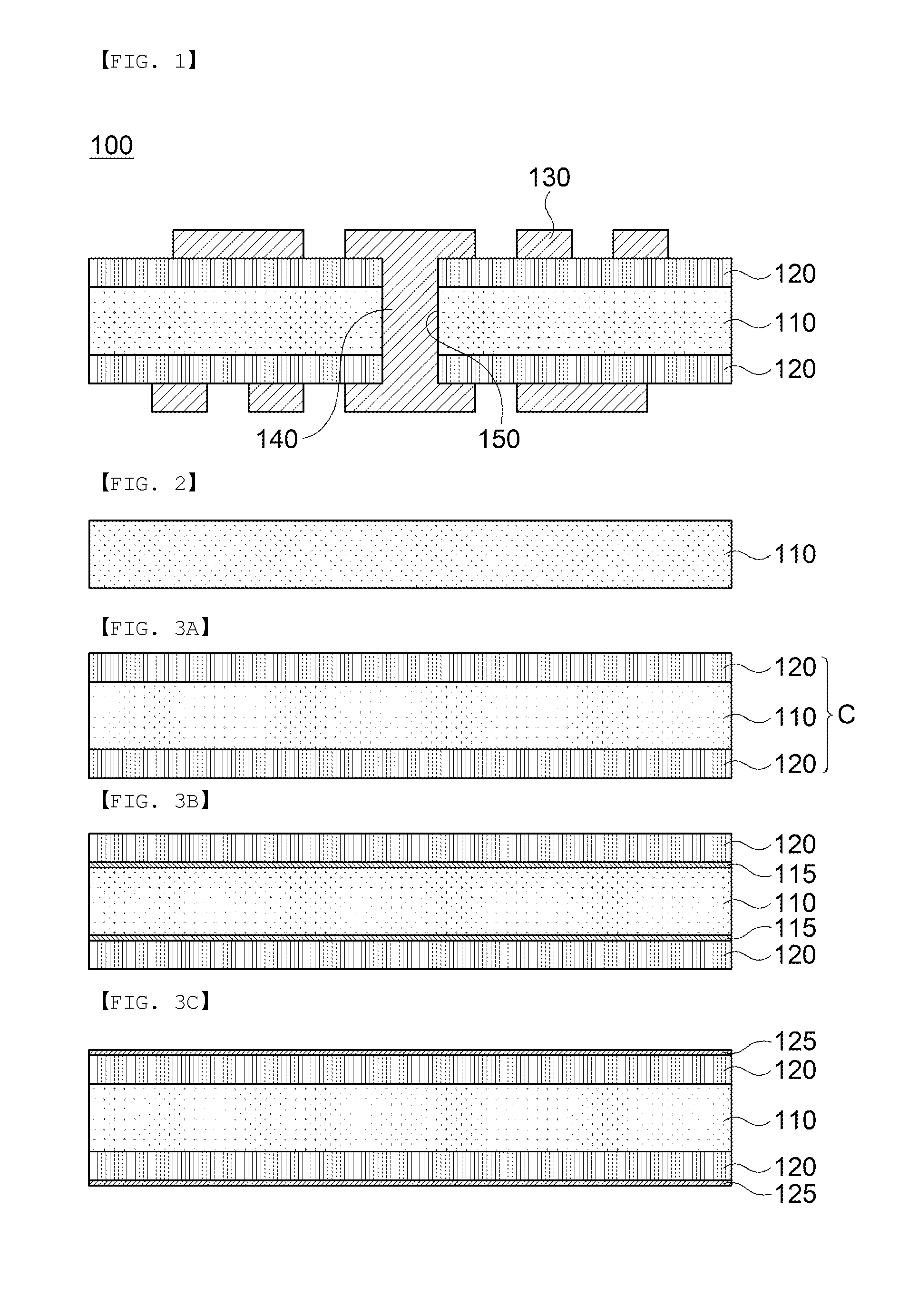
[0066]First, as illustrated in FIG. 2, the core reinforcement 110 is prepared. The core reinforcement 110 may be a plate-shaped glass or a non-conductive polymer material. In the case of the non-conductive polymer material, the core reinforcement may be formed in a film type.

[0067]Herein, in the case of glass, the core reinforcement 110 preferably has the elastic module of 50 GPa or more and is formed at a thickness of 25 to 200 μm and when the thickness is maintained, the core reinforcement may be deformed with a predetermined radius of curvature and then may be recovered to an original state without being damaged, during the process of manufacturing a printed circuit board.

[0068]Next, as illustrated in FIG. 3A, the core C may be manufactured by forming ...

second exemplary embodiment

Method For Manufacturing Printed Circuit Board

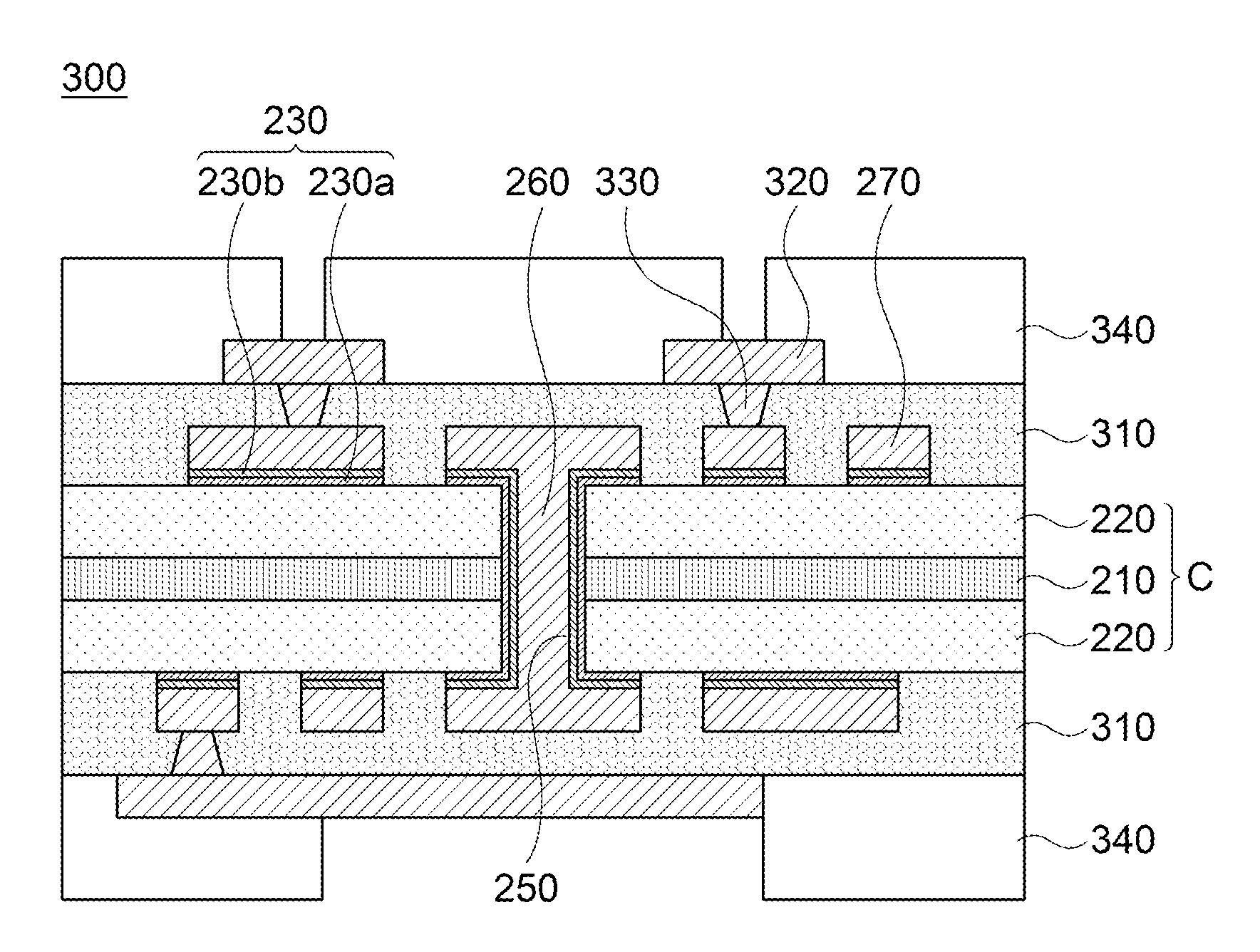
[0089]Next, FIGS. 7 to 12 are process cross-sectional views sequentially illustrating a method for manufacturing a printed circuit board according to a second exemplary embodiment of the present invention.

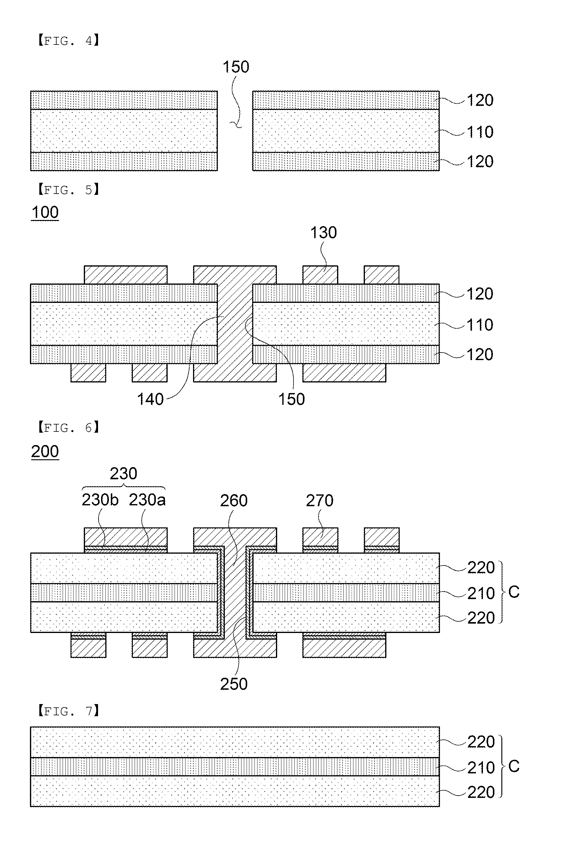
[0090]First, as illustrated in FIG. 7, the core C may be manufactured by bonding the core reinforcements to the upper and lower surfaces of the insulating layer 210. In this case, the insulating layer 210 may be made of an insulating material impregnated with a glass fabric as a polymer material having heat resistance and may be formed of a film type or an insulating sheet with which the glass fabric is mixed. Further, the insulating layer 210 laminated between the core reinforcements absorbs impact that occurs during the process to prevent the core reinforcements 220 from being damaged due to impact or warpage.

[0091]The manufacturing of the core C may further include laminating the core reinforcements 220 on both surfaces of the insula...


PUM

PropertyMeasurementUnit
thicknessaaaaaaaaaa
thicknessaaaaaaaaaa
thicknessaaaaaaaaaa

Abstract

Disclosed herein are a printed circuit board and a method for manufacturing the same. The printed circuit board includes: a core reinforcement having stiffness; insulating layers formed on both surfaces of the core reinforcement; a through hole formed by penetrating through the insulating layer and the core reinforcement; and a circuit layer formed on the insulating layer and a plating layer formed in the through hole for implementing inter-layer connection of the circuit layers.

Description

[0001]This application claims the benefit under 35 U.S.C. Section 119 of Korean Patent Application Serial Nos. 10-2012-0083160, 10-2012-0140480, and 10-2013-0061168 entitled “Printed Circuit Board And Method For Manufacturing The Same” filed on Jul. 30, 2012, Dec. 5, 2012 and May 29, 2013, which is hereby incorporated by reference in its entirety into this application.BACKGROUND OF THE INVENTION[0002]1. Technical Field[0003]The present invention relates to a printed circuit board and a method for manufacturing the same.[0004]2. Description of the Related Art[0005]In recent, as a thickness of portable devices have become thin, attempts to reduce a thickness of all the internal components by making a board having a plurality of electronic components mounted thereon thin and making electronic components mounted in the portable devices thin have been conducted.[0006]In particular, when the board having the electronic components mounted thereon is manufactured in a thin plate type, the b...

Claims


Application Information

Patent Timeline
Patent Type & Authority Applications(United States)
IPC IPC(8): H05K1/02H05K3/00H05K3/10
CPCH05K1/0271H05K3/0094H05K3/10H05K3/4602H05K3/4605H05K2201/0195H05K2201/029H05K2201/068H05K2201/09536
Inventor MIN, TAE HONGCHO, SUK HYEONKIM, JONG RIPLEE, JUNG HAN
Owner SAMSUNG ELECTRO MECHANICS CO LTD
Why Eureka
Try Eureka