Semiconductor device and method for manufacturing semiconductor device

Inactive Publication Date: 2014-02-06
MITSUBISHI ELECTRIC CORP
View PDF15 Cites 23 Cited by
  • Summary
  • Abstract
  • Description
  • Claims
  • Application Information

AI Technical Summary

Benefits of technology

[0011]In the semiconductor device according to the present invention, a part of the spherical outer shape of each of the plurality of spherical particles is buried in the other surface of the metal plate. Therefore, the plurality of spherical particles cut into the other surface of the metal plate, and thus, the plurality of spherical particles can be strongly joined to the metal plate. In addition, a contact area between each of the plurality of spherical particles and the metal plate can be increased. Therefore, peel-off of the plurality of spherical particles from the metal plate can be suppressed. Accordingly, heat of the semiconductor element can be dissipa

Problems solved by technology

If the protrusion is peeled off from the mounting plate, it becomes difficult to efficiently transfer heat from the electronic equipment serving as the heat generating body

Method used


Image

  • Semiconductor device and method for manufacturing semiconductor device
  • Semiconductor device and method for manufacturing semiconductor device
  • Semiconductor device and method for manufacturing semiconductor device

Examples


case 5

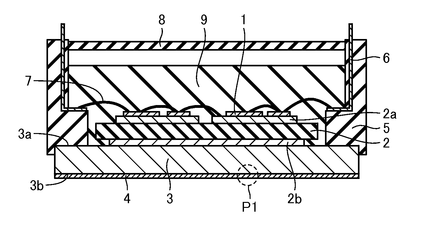
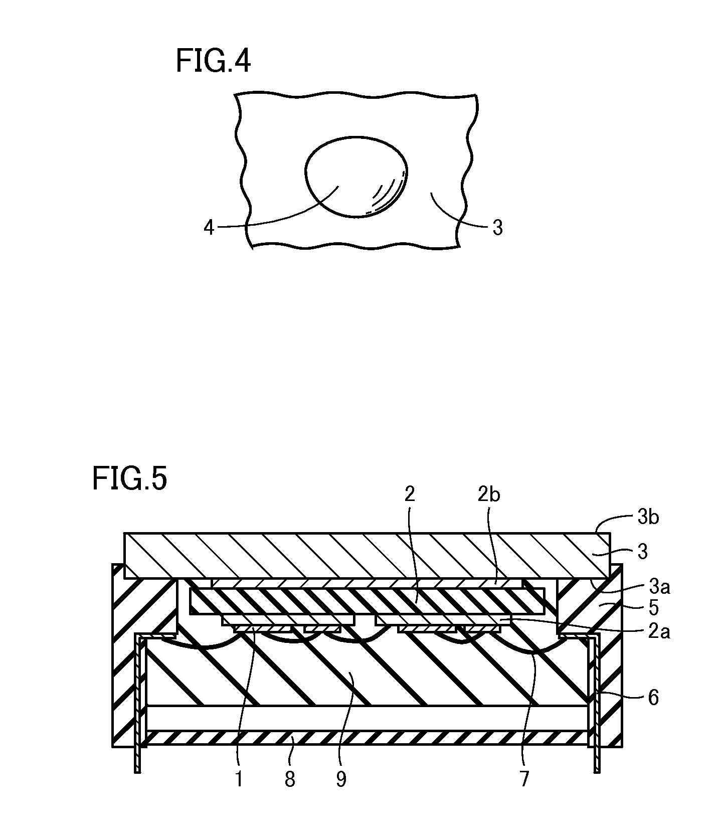
[0031]Case 5 is formed around one surface 3a of metal plate 3. Case 5 is made of, for example, a resin. Electrode terminal 6 is attached to case 5. Electrode terminal 6 is formed to protrude outward from case 5. Wire 7 is, for example, an aluminum wire. Semiconductor elements 1 are electrically connected by wire 7. Semiconductor element 1 and electrode terminal 6 attached to case 5 are also electrically connected by wire 7. Lid 8 is placed at an upper end of case 5. Lid 8 is for preventing entry of dust and water.

[0032]Semiconductor element 1, substrate 2 and wire 7 are disposed in an internal space surrounded by metal plate 3, case 5 and lid 8. In the internal space, semiconductor element 1, substrate 2 and wire 7 are covered with sealing resin 9. Sealing resin 9 is, for example, a silicone gel.

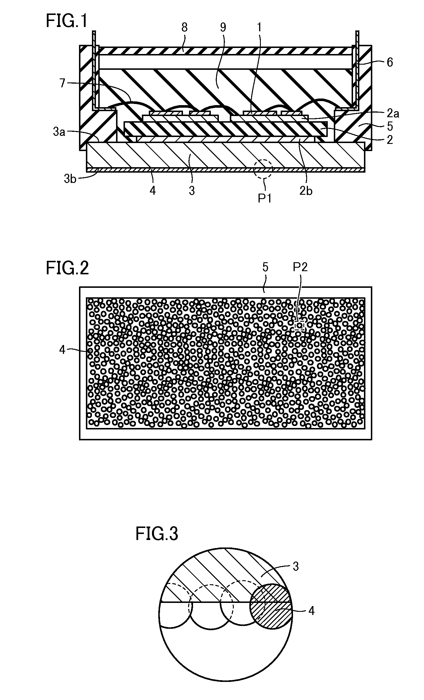
[0033]The plurality of spherical particles 4 will be described in more detail with reference to FIGS. 3 and 4. Each of the plurality of spherical particles 4 has a spherical outer shape. A p...


PUM


Abstract

A semiconductor device includes: a semiconductor element; a substrate; a metal plate; and a plurality of spherical particles. The substrate has the semiconductor element mounted thereon. The metal plate has one surface and the other surface that face each other, and the substrate is provided on the one surface. The plurality of spherical particles each has a spherical outer shape, and a part of the spherical outer shape is buried in the other surface of the metal plate. With such a configuration, there can be obtained a semiconductor device that allows promotion of heat dissipation from the semiconductor element, and a method for manufacturing the semiconductor device.

Description

BACKGROUND OF THE INVENTION[0001]1. Field of the Invention[0002]The present invention relates to a semiconductor device and a method for manufacturing the semiconductor device.[0003]2. Description of the Background Art[0004]In a semiconductor device, a heat dissipating device such as a heat sink is used to promote heat dissipation from a heat generating body such as a semiconductor element. There has been proposed a structure for efficiently transferring heat from the heat generating body such as the semiconductor element to the heat sink to promote heat dissipation from the heat generating body such as the semiconductor element.[0005]Japanese Patent Laying-Open No. 2006-134989, for example, discloses a structure capable of reducing a thermal resistance between electronic equipment and a heat sink. In this structure, a protrusion that is deformed by press contact is arranged on a bottom surface of a mounting plate of the electronic equipment on the side where the heat sink is attach...

Claims


Application Information

Patent Timeline
IPC IPC(8): H01L23/36H01L21/50
CPCH01L21/50H01L23/36H01L23/367H01L23/3735H01L23/3736H01L23/49811H01L25/072H01L2224/45124H01L2224/48137H01L2224/48227H01L2924/16195H01L23/053H01L2924/3025H01L2924/181H01L2924/00H01L2924/00012
Inventor OKA, SEIJIYAMAGUCHI, YOSHIHIRO
Owner MITSUBISHI ELECTRIC CORP
Why Eureka
Try Eureka