Low power scan flip-flop cell

a flip-flop cell, low-power scanning technology, applied in the direction of electronic circuit testing, measurement devices, instruments, etc., can solve the problems of high power consumption, high power consumption may exceed the circuit's power rating, and high power consumption may be much greater, so as to reduce unnecessary power consumption and eliminate unnecessary switching

Active Publication Date: 2014-02-06
NXP USA INC
View PDF4 Cites 32 Cited by
  • Summary
  • Abstract
  • Description
  • Claims
  • Application Information

AI Technical Summary

Benefits of technology

[0007]According to the invention, the low power scan flip-flop cell prevents the Q output signal from changing state during the scan shift operation to eliminate unnecessary switching of the comb

Problems solved by technology

For a full scan design, during scan testing, all of the flip-flops and all of the combinational logic connected to the flip-flops, may be toggling at the same time, causing very high power consumption.
This high power consumption is much greater than the power consum

Method used


Image

  • Low power scan flip-flop cell
  • Low power scan flip-flop cell
  • Low power scan flip-flop cell

Examples


first embodiment

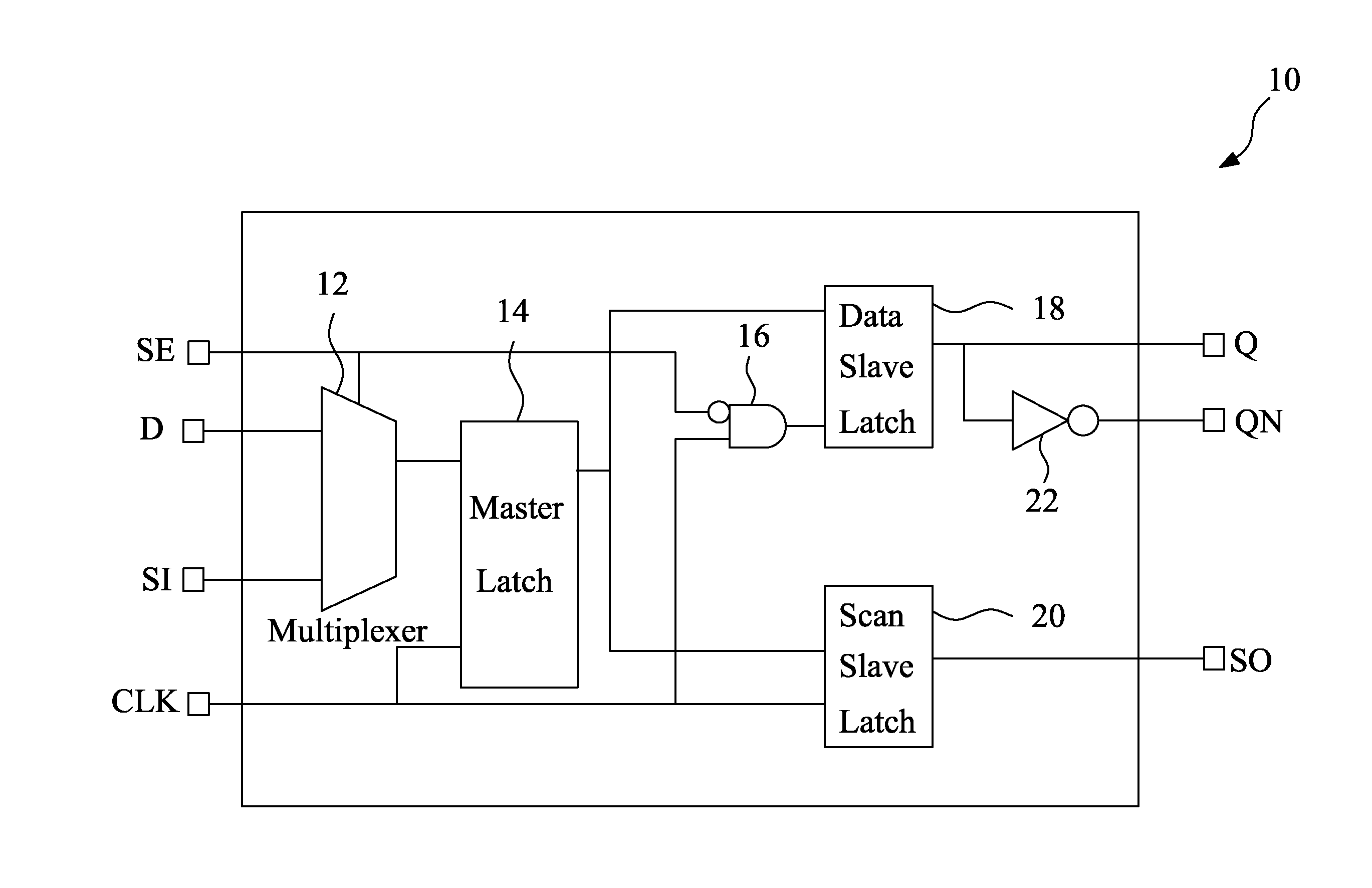
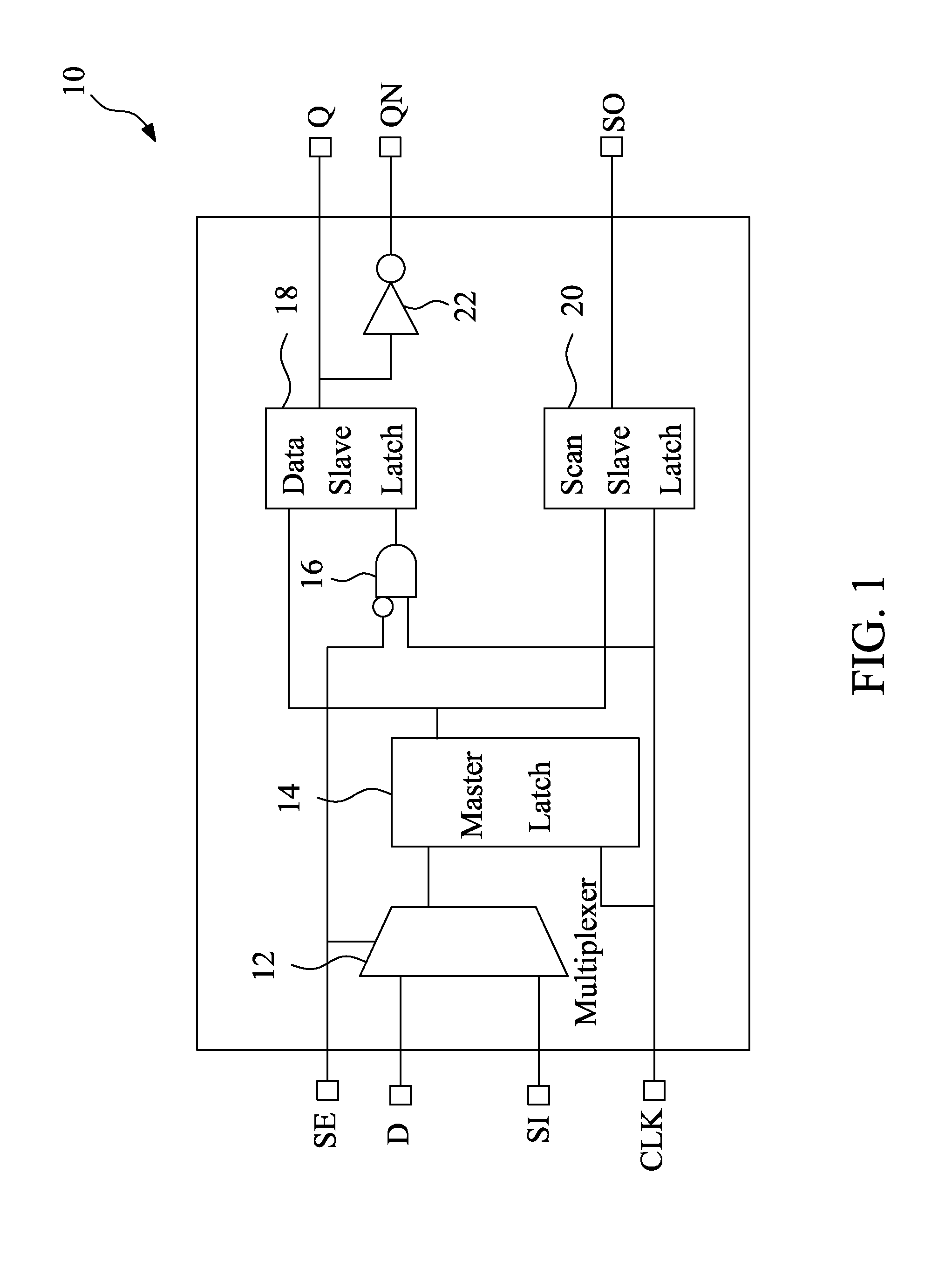
[0018]Referring now to FIG. 1, a schematic block diagram of a low power scan flip-flop cell 10 in accordance with the present invention is shown. The scan flip-flop cell 10 includes a multiplexer 12, a master latch 14, a first logic gate 16, a data slave latch 18, a scan slave latch 20, and a second logic gate 22.

[0019]The multiplexer 12 receives as inputs a data input (D) signal and a scan input (SI) signal, and outputs a first data signal depending on a scan enable (SE) input signal. The master latch 14 is connected to the multiplexer 12 and receives the first data signal at a data input and a clock signal (CLK) at a clock input, and outputs a first latch signal. The scan slave latch 20 is connected to the master latch 14, and receives the first latch signal at a data input and generates a scan output (SO) signal. The CLK signal also is input to the scan slave latch 20 at its clock input.

[0020]In this embodiment, the first logic gate 16 comprises an AND gate that receives as input...

second embodiment

[0031]Referring to FIG. 4b, when the scan flip-flop cell 30′ is in scan mode, the SE signal is at logic high and the inverted scan enable (SEb) signal is at logic low. Therefore, the second transistor 52 is switched on. The signal “qb” at the first connection node goes high during scan shift so as to keep the Q output signal at a logic low state. However, when the scan flip-flop cell 30′ is in functional mode, the second transistor 52 is switched off and so does not hold the “qb” signal high. Meanwhile, as discussed above with reference to the second embodiment, the first transistor 38 is switched on and the first tri-state inverter 32 operates under the control of the clock signal during the functional mode. Therefore, the data slave latch 18′ will output the Q and QN signals based on the first latch signal from the master latch 14 and the clock signal.

fourth embodiment

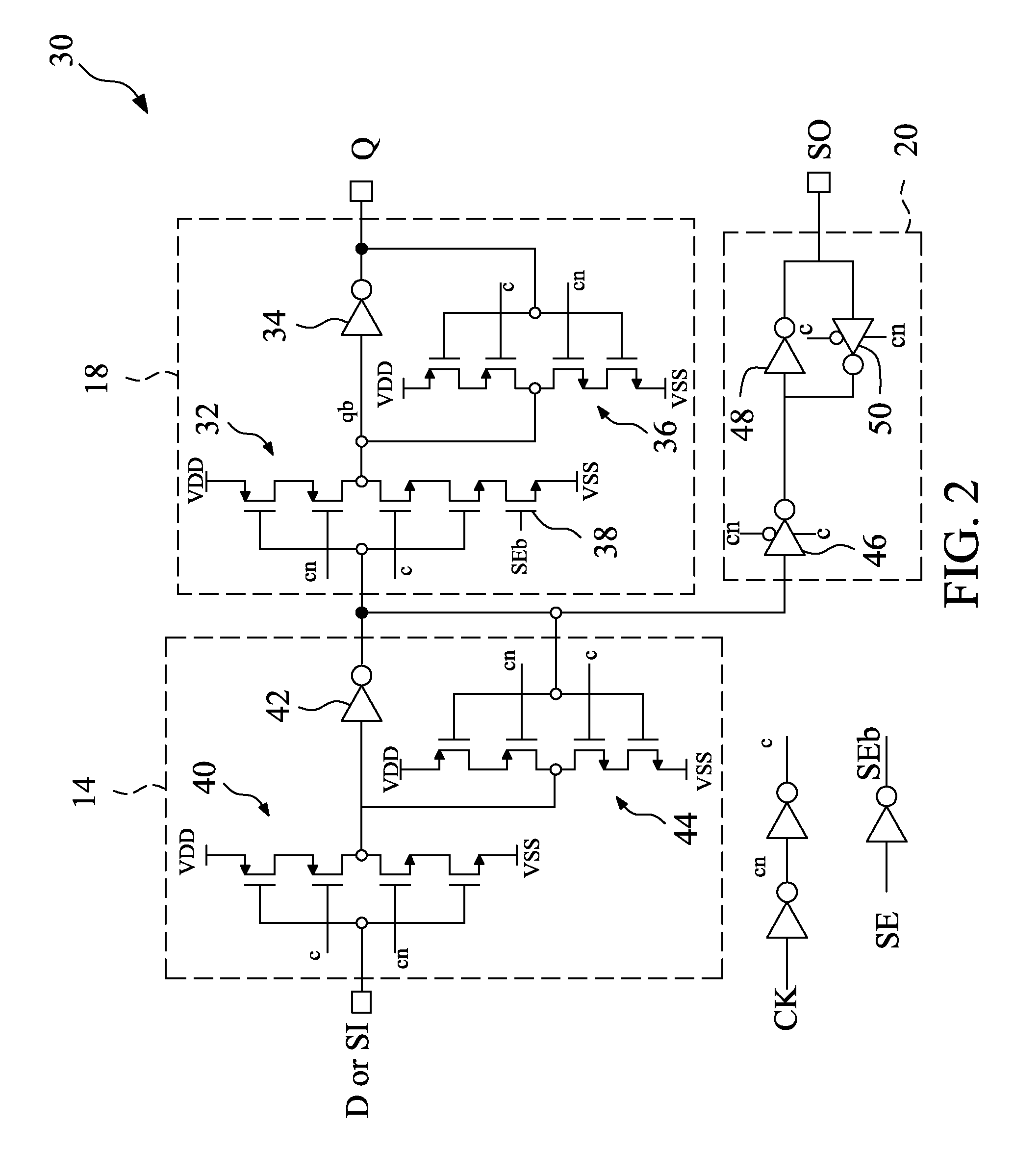
[0032]FIG. 5 is a schematic circuit diagram of a low power scan flip-flop cell 54 in accordance with the present invention. The scan flip-flop cell 54 includes a multiplexer (not shown), a master latch 14, a data slave latch 58, and a scan slave latch 60. In this embodiment, the master latch 14 is similar to the master latch 14 shown in FIGS. 2 and 3, so a detailed description thereof is not repeated.

[0033]The data slave latch 58 includes a first transmission gate 62, a fourth normal inverter 64 and a seventh tri-state inverter 66. The fourth normal inverter 64 and seventh tri-state inverter 66 are connected in a loop. The first transmission gate 62 receives the first latch signal from the master latch 14 as an input and has an output connected to a first connection node (QN) located between an input of the fourth normal inverter 64 and an output of the seventh tri-state inverter 66. The Q output is generated at a second connection node located between an output of the fourth normal...


PUM


Abstract

A low power scan flip-flop cell includes a multiplexer, a master latch, a scan slave latch and a data slave latch. The master latch is connected to the multiplexer, and used for generating a first latch signal. The scan slave latch is connected to the master latch, and generates a scan output (SO) signal. The data slave latch is connected to the master latch, and generates a Q output depending on a scan enable (SE) input signal and the first latch signal. The Q output is maintained at a predetermined level during scan mode, which eliminates unnecessary switching of combinational logic connected to the scan flip-flop cell and thus reduces power consumption.

Description

BACKGROUND OF THE INVENTION[0001]The present invention relates to testing integrated circuits and, more particularly, to a low power scan flip-flop cell.[0002]Scan chains comprise a plurality of interconnected scan flip-flops and are used to obtain access to internal nodes of an integrated circuit (IC) to simplify testing of the IC by passing test data through the flip-flops. The scan flip-flop is configured to operate in one of two modes, functional mode and scan mode.[0003]When the scan enable input of a scan flip-flop is set to logic low, the scan flip-flop is in the functional mode; when the scan enable input of the scan flip-flop is set to logic high, the scan flip-flop is in scan mode (in this example, the scan enable signal is high active). For a full scan design, during scan testing, all of the flip-flops and all of the combinational logic connected to the flip-flops, may be toggling at the same time, causing very high power consumption. This high power consumption is much g...

Claims


Application Information

Patent Timeline
IPC IPC(8): G01R31/3177
CPCG01R31/318541
Inventor ZHANG, WANGGENLU, SIANZHANG, SHAYAN
Owner NXP USA INC
Why Eureka
Try Eureka