Supercharge Your Innovation With Domain-Expert AI Agents!

Method and system for manufacturing optical display panel

a technology of optical display panel and manufacturing method, which is applied in the direction of instruments, polarizing elements, other domestic articles, etc., can solve the problems of easy damage to the optical display panel, and the hydrophilicity of the pva film used as the base material of the polarizing film is very high, so as to suppress wrinkles and bubbles, and travel accurately

Inactive Publication Date: 2014-02-13
NITTO DENKO CORP
View PDF2 Cites 8 Cited by
  • Summary
  • Abstract
  • Description
  • Claims
  • Application Information

AI Technical Summary

Benefits of technology

The patent text describes a method for making optical display panels continuously. The method involves controlling the movement of an optical film very precisely to avoid wrinkles and bubbles during the process of bonding it to a liquid crystal cell. This is achieved by using a large number of devices to control the film's travel. Additionally, the length of the film wound into a roll is increased to improve productivity and reduce losses caused by replacing the roll.

Problems solved by technology

However, as the length of the long film increases, namely, as the diameter of the roll increases, displacement of windings becomes more likely to occur due to vibration during transportation or other causes.
The PVA film used as a base material for the polarizing film has very high hydrophilicity and, in general, is easily affected by moisture or heat.
When a long film is unwound from a roll with displaced windings in a conventional continuous manufacturing method, the displacement of windings can degrade the straight travel of the film, so that bonding misalignment or bubbles can easily occur at or around the displaced winding, which may cause defects.

Method used


Image

  • Method and system for manufacturing optical display panel
  • Method and system for manufacturing optical display panel
  • Method and system for manufacturing optical display panel

Examples


example 1

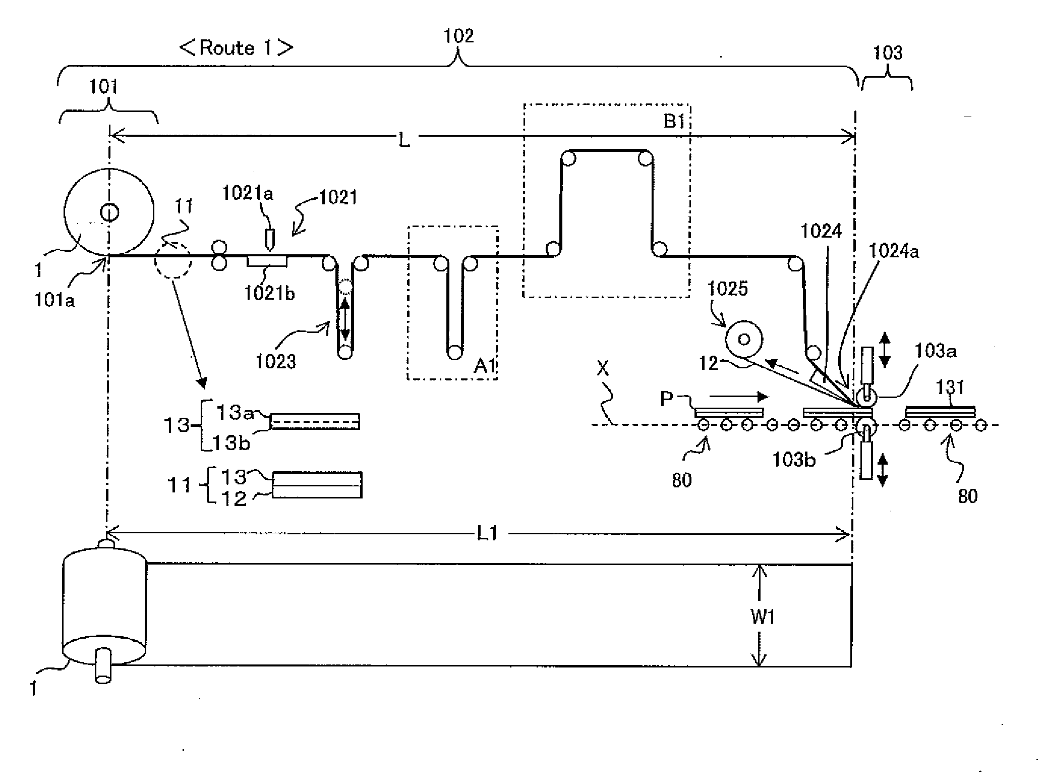
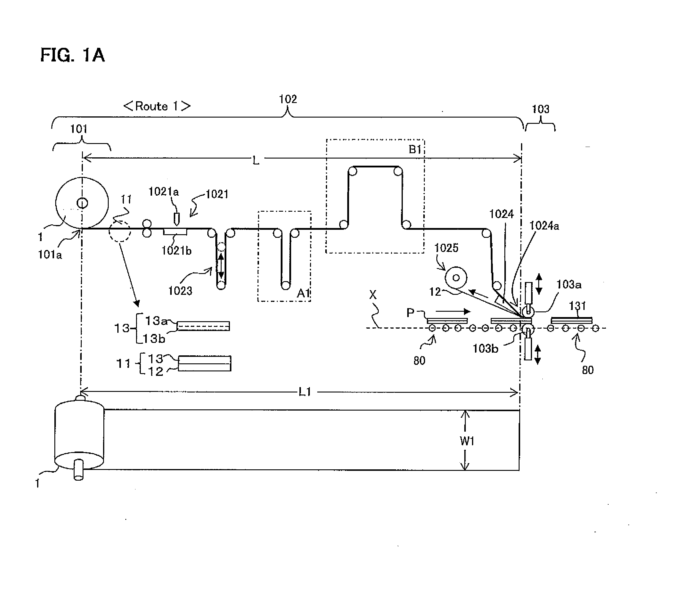
[0113]Using the roll of long polarizing film with a width (W) of 65 cm (the roll having displaced windings), a laminate sample was prepared by bonding the polarizing film piece to the glass plate in the manufacturing system of FIG. 1A. The number n of the prepared samples was 50. In the cutting unit, the polarizing film was cut at intervals of 100 cm in the longitudinal direction. The resulting polarizing film piece was bonded to the central part of the glass plate with a length of 102 cm and a width of 67 cm. In this process, the length L of the film in the route was 10.5 m, and L / W was 16.2 (rounded to one decimal place).

example 2

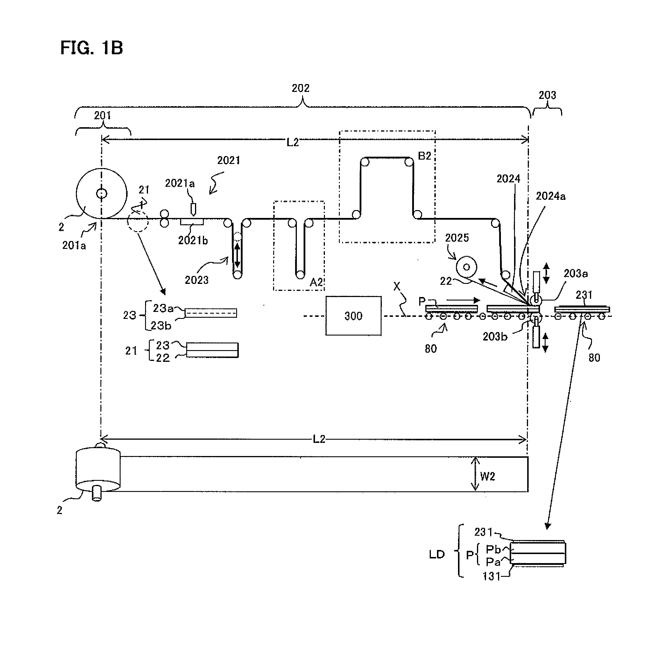
[0114]The same procedure as in Example 1 was performed except that the manufacturing system of FIG. 2 was used. The length L of the film in the route was 12.5 m, and L / W was 19.2.

example 3

[0115]The same procedure as in Example 1 was performed except that the manufacturing system of FIG. 3 was used. The length L of the film in the route was 13.6 m, and L / W was 20.9.


PUM

PropertyMeasurementUnit
wavelengthaaaaaaaaaa
angleaaaaaaaaaa

Abstract

Manufacturing method is for manufacturing an optical display panel including an optical cell and a pressure-sensitive adhesive layer-carrying optical film provided thereon with the pressure-sensitive adhesive layer interposed therebetween, which includes the steps of unwinding a multilayer optical film from a roll, feeding the multilayer optical film, feeding an optical cell, peeling off the optical film from a carrier film, and bonding the optical film to one side of the optical cell with a pressure-sensitive adhesive interposed therebetween, wherein the longitudinal length (L) of the carrier film between a position at which the multilayer optical film begins to be unwound in the film feeding step and a position at which peeling is started in the peeling step is 15 times or more the width (W) of the carrier film.

Description

BACKGROUND OF THE INVENTION[0001]1. Field of the Invention[0002]The invention relates to a method and a system for manufacturing an optical display panel including an optical cell, such as a liquid crystal cell or an electroluminescent (EL) display cell, and an optical film provided on the surface of the optical cell.[0003]2. Description of the Related Art[0004]One of liquid crystal display (LCD) device manufacturing steps includes a bonding step in which multilayer optical films each having a polarizing film are bonded to both sides of a liquid crystal cell, which includes a pair of substrates and a liquid crystal layer sandwiched therebetween. In general, such multilayer optical films include a polarizing film and an adhesive or pressure-sensitive adhesive layer formed on at least one surface of the polarizing film, and thus can be bonded to the surface of a liquid crystal cell with the adhesive or pressure-sensitive adhesive interposed therebetween.[0005]A method used for bonding...

Claims


Application Information

Patent Timeline
Patent Type & Authority Applications(United States)
IPC IPC(8): G02B5/30H10K99/00
CPCG02B5/3025G02F1/1303G02F1/133528G02F2202/28B29C65/4825B29C65/5057B29C65/7861B29C66/1122B29C66/45B29C66/7338B29C66/83221B29C66/83413B29L2031/3475B29C65/7891B29C66/71B29C2793/0081B32B37/18B32B38/18B32B2457/202B65H2301/51122B65H2301/5162B65H2801/61B65H29/54Y10T156/1705B65H2515/84H10K71/80H10K71/00H10K71/50B29K2029/04G02F1/1335G02F1/13G02B5/30B65H39/16
Inventor UMEMOTO, SEIJIKIMURA, KOUJINAKAZONO, TAKUYAHADA, KAZUYA
Owner NITTO DENKO CORP
Features
  • R&D
  • Intellectual Property
  • Life Sciences
  • Materials
  • Tech Scout
  • Unparalleled Data Quality
  • Higher Quality Content
  • 60% Fewer Hallucinations
Learn More