Optoelectronic integrated package module

a technology of integrated package module and optoelectronic, applied in the direction of optical elements, instruments, optics, etc., can solve the problems of electromagnetic noise interference and transmission loss

Inactive Publication Date: 2014-02-13
KK TOSHIBA
View PDF2 Cites 24 Cited by
  • Summary
  • Abstract
  • Description
  • Claims
  • Application Information

AI Technical Summary

Problems solved by technology

This arises the problems of transmission loss and electromagnetic noise interference.

Method used


Image

  • Optoelectronic integrated package module
  • Optoelectronic integrated package module
  • Optoelectronic integrated package module

Examples


first embodiment

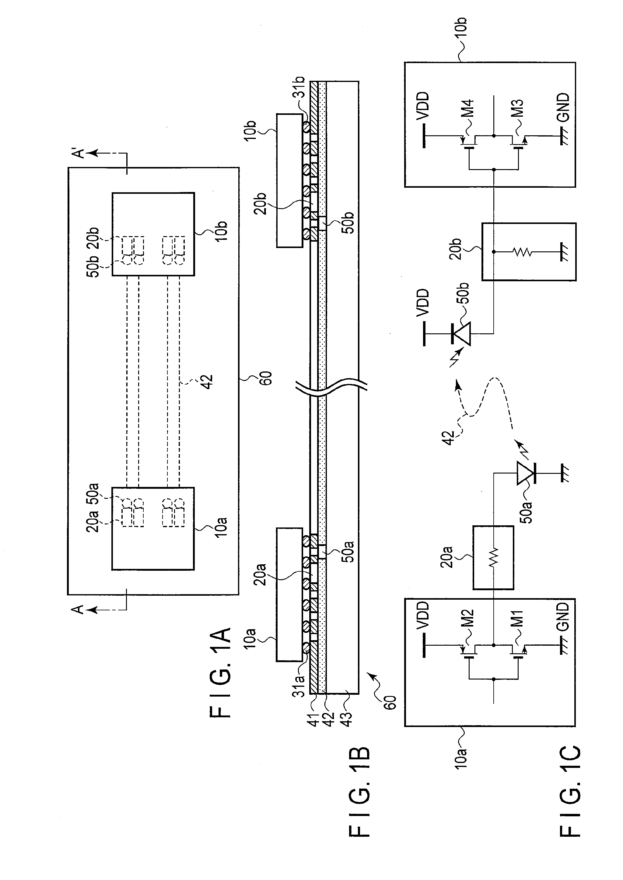
[0024]FIGS. 1A to 1C are views for explaining the schematic arrangement of an optoelectronic integrated package module according to the first embodiment. FIG. 1A is a plan view of the optoelectronic integrated package module. FIG. 1B is a sectional view taken along A-A′ in FIG. 1A. FIG. 10 is a circuit diagram of the optoelectronic integrated package module.

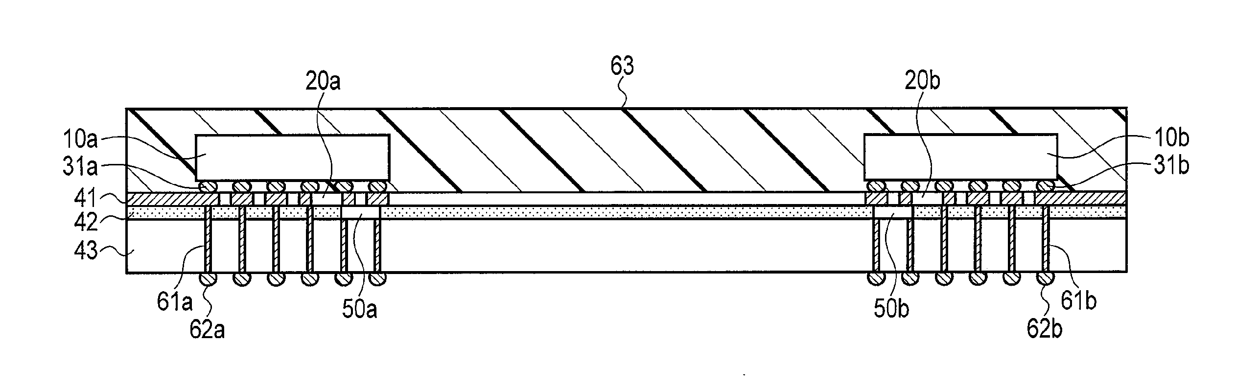
[0025]The optoelectronic integrated package module according to this embodiment is formed by mounting semiconductor integrated circuit chips 10, i.e., 10a and 10b, on a silicon interposer 60 including a silicon substrate 43, electrical circuit elements 20, i.e., 20a and 20b, electrical interconnections 41, optical waveguides 42, and optical semiconductor elements 50, i.e., 50a and 50b.

[0026]The optical semiconductor elements 50 are arranged on the silicon substrate 43 of the silicon interposer 60 so as to be spaced apart from each other. One of the optical semiconductor elements 50 is the light-emitting element 50a, and the othe...

second embodiment

[0068]FIGS. 7A, 7B, and 7C are views for explaining the schematic arrangement of an optoelectronic integrated package module according to the second embodiment. FIG. 7A is a plan view of the optoelectronic integrated package module. FIG. 7B is a sectional view taken along A-A′ in FIG. 7A. FIG. 7C is a circuit diagram showing the optoelectronic integrated package module on the transmission side. Note that the same reference numbers as in FIGS. 1A, 1B, and 1C denote the same parts in FIGS. 7A, 7B, and 7C, and a detailed description of them will be omitted.

[0069]This embodiment differs from the first embodiment described above in the arrangement of electrical circuit elements 20. The electrical circuit element 20 in this embodiment is not a simple thin film resistive element but is a driver IC (driver circuit element) or receiver IC (receiver circuit element) having a size of 12 mm×12 mm and a thickness of 50 μm, which is manufactured by, for example, a 90 nm generation CMOS process. T...

third embodiment

[0088]FIGS. 10A and 10B are views for explaining the schematic arrangement of an optoelectronic integrated package module according to the third embodiment. FIG. 10A is a plan view. FIG. 10B is a sectional view taken along A-A′ in FIG. 10A. Note that the same reference numbers as in FIGS. 1A and 1B denote the same parts in FIGS. 10A and 10B, and a detailed description of them will be omitted.

[0089]In the optoelectronic integrated package module shown in FIGS. 1A and 1B, the semiconductor integrated circuit chips 10 are mounted on the silicon interposer 60 so as to overlap the optical semiconductor elements 50 when viewed from above. In contrast to this, in this embodiment, as shown in FIGS. 10A and 10B, optical semiconductor elements 50 are arranged outside semiconductor integrated circuit chips 10 when viewed from above. This facilitates heat dissipation from the optical semiconductor elements 50. In this case, in order to sufficiently reduce the influences of attenuation in transm...


PUM


Abstract

According to one embodiment, there is provided an optoelectronic integrated package module including a silicon interposer that has an electrical interconnection and an optical waveguide, and formed on a silicon substrate, an optical semiconductor element formed in the silicon interposer, and electrically connected to the electrical interconnection and optically coupled to the optical waveguide, an electrical circuit element formed in the silicon interposer, and electrically connected to the optical semiconductor element, and a semiconductor integrated circuit chip mounted on the silicon interposer, and electrically connected to the electrical circuit element. The semiconductor integrated circuit chip transmits an electrical signal to the optical semiconductor element via the electrical circuit element or receives an electrical signal from the optical semiconductor element via the electrical circuit element.

Description

CROSS-REFERENCE TO RELATED APPLICATIONS[0001]This application is based upon and claims the benefit of priority from Japanese Patent Application No. 2012-179447, filed Aug. 13, 2012, the entire contents of which are incorporated herein by reference.FIELD[0002]Embodiments described herein relate generally to an optoelectronic integrated package module.BACKGROUND[0003]Recently, with improvements in the performance of electronic devices and increases in the volume of multimedia contents, the amount of signal processing in information communication devices has increased. With this increase, the signal transmission rates of interconnections inside and outside electronic devices have increased. This arises the problems of transmission loss and electromagnetic noise interference. A great deal of attention has therefore been paid to optical signal transmission having features of being high-speed and low in noise, and various types of optoelectronic integrated package modules have been propos...

Claims


Application Information

Patent Timeline
Patent Type & Authority Applications(United States)
IPC IPC(8): H01L31/12
CPCH01L31/12G02B6/4274G02B6/428G02B6/43H01L2224/16225H01L2924/13091H01L2924/00
Inventor UEMURA, HIROSHIFURUYAMA, HIDETO
Owner KK TOSHIBA
Why Eureka
Try Eureka