Light emitting device and method for manufacturing same

a technology manufacturing methods, which is applied in the testing/measurement of individual semiconductor devices, semiconductor/solid-state devices, instruments, etc., can solve the problems of poor yield, high material cost, and high cost of light emitting devices (white led devices). , to achieve the effect of saving fluorescent materials, reducing costs, and improving chromaticity variations

Inactive Publication Date: 2014-02-13
ELM CO LTD
View PDF4 Cites 21 Cited by
  • Summary
  • Abstract
  • Description
  • Claims
  • Application Information

AI Technical Summary

Benefits of technology

[0059]The light emitting device according to the present invention is able to solve all the problems described above, with a chip-size package structure including a reflection wall. Specifically, the following is achieved.
[0060]Since an expensive package substrate is not used, it is possible to reduce the cost.
[0061]A white light emitting element is provided in which the fluorescent material-containing film piece is overlaid on the light extraction surface of the semiconductor light emitting element, and it is possible to save the fluorescent material and to improve variations of chromaticity depending on a viewing angle due to a white point light emitter.
[0062]The surface other than the bump mounting surface of the semiconductor light emitting element and the light exit surface of the fluorescent material-containing film piece is covered with the reflection wall, and light traveling in a direction other than a direction toward the light exit surface (particularly, light traveling toward the side surface of the semiconductor light emitting element, light traveling toward the side surface of the fluorescent material-containing film piece, etc.) is dispersed and reflected by the reflection wall and condensed in a specific direction.
[0063]Moreover, the reflection wall is formed so as to be in close contact with a light source (namely, at the closest distance therefrom), and thus is able to most efficiently reflect and condense light in dispersion and reflection, whereby it is possible to provide high brightness.
[0064]Furthermore, since the semiconductor light emitting element is mounted at its bump mounting surface on the external substrate, heat is radiated from the semiconductor light emitting element directly to the bump, a solder, and the external substrate.

Problems solved by technology

The other reason is that a light emitting device (white LED device) itself is expensive.
The reasons for making a white LED device expensive are that the material cost is high and the yield is poor.
With such a manufacturing method, when a light emitting device is determined as being not good in a chromaticity test, the entire light emitting device including the package is determined as being not good, and even the most-expensive package is discarded.
In this case, it is possible to conduct the chromaticity test at the stage of chip, and thus an expensive package is no longer discarded.
However, the light emitting device 147 with such a structure lacks an important characteristic required for an environmentally friendly lamp.

Method used


Image

  • Light emitting device and method for manufacturing same
  • Light emitting device and method for manufacturing same
  • Light emitting device and method for manufacturing same

Examples


first embodiment

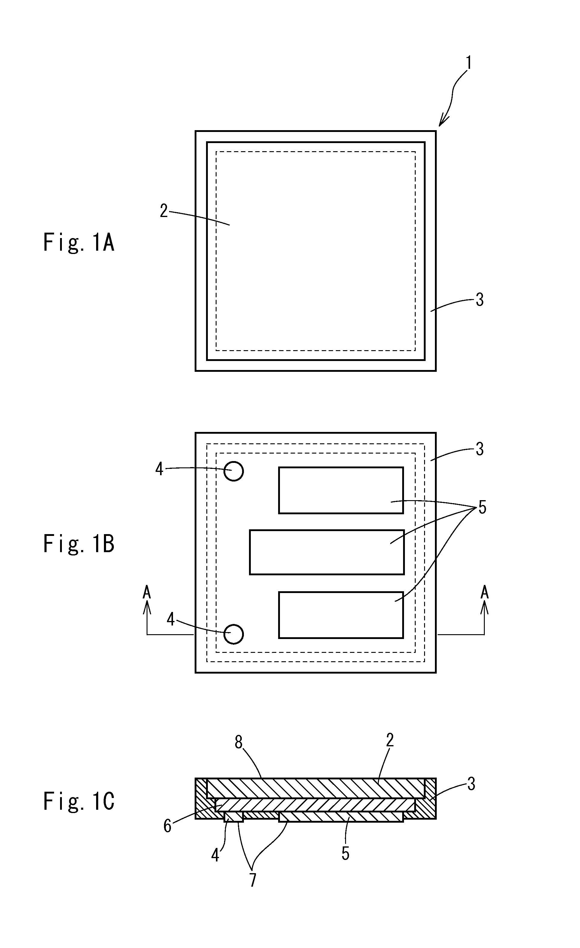
[0085]First, FIG. 1A to 1C show a light emitting device according to the In addition, a manufacturing method thereof includes steps as shown in FIGS. 5A to 5F and is a manufacturing method in which a plurality of light emitting devices 1 are manufactured together.

[0086]In this case, as shown in FIGS. 1A to 1C, the light emitting device 1 includes a semiconductor light emitting element 6 in which bumps 4 and 5 having a thickness of 15 μm are formed on an n-side electrode and a p-side electrode of a blue LED element which emits blue light; a fluorescent material-containing film piece 2 which is integrated on a light extraction surface of the semiconductor light emitting element 6 by an adhesive and contains a fluorescent material; and a reflection wall 3 which covers an exposed surface other than: bump end portions 7 which are mounting surfaces of the semiconductor light emitting element 6; and a light exit surface 8 of the fluorescent material-containing film piece which is a light ...

second embodiment

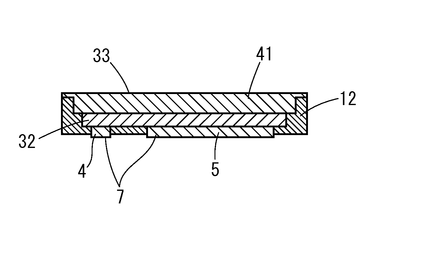
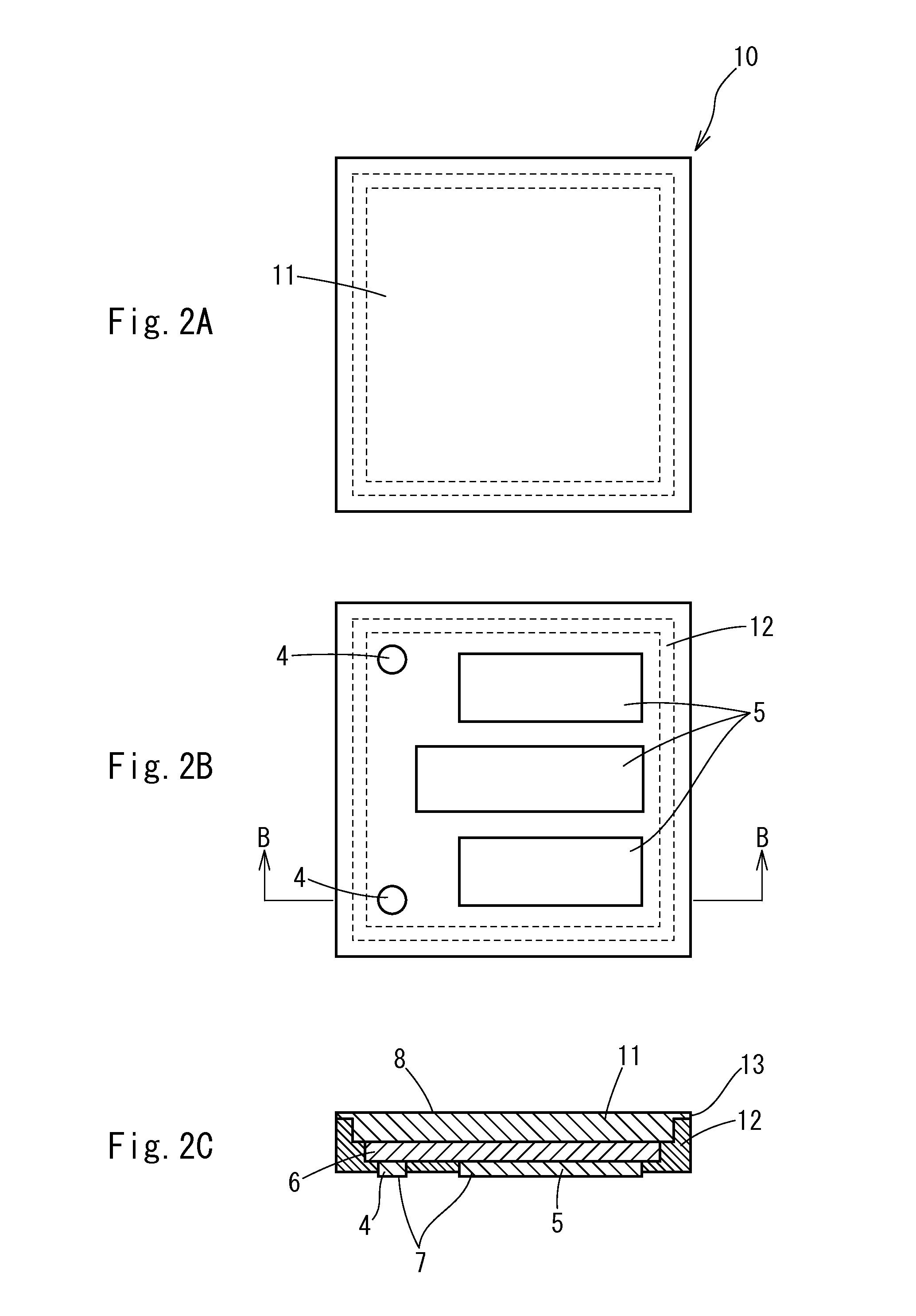
[0100]Next, FIGS. 2A to 2C show a light emitting device according to a In addition, FIGS. 6A to 6E show a manufacturing method thereof.

[0101]In this case, as shown in FIGS. 2A to 2C, the light emitting device 10 is almost the same as that in the first embodiment, but is different therefrom in being slightly subjected to structural constraints in order to simplify the manufacturing method. This is that a portion 13 at which no reflection wall is present occurs at a part of the side surface of a fluorescent material-containing film piece. Thus, there is the possibility that slight light leaks laterally, but the above-described problems are almost solved similarly to the light emitting device 1 according to the first embodiment.

[0102]The method for manufacturing the light emitting device 10 includes steps in FIGS. 6A to 6E. Most of the steps are the same as those of the manufacturing method in FIG. 5A, and FIG. 5C to 5F and the description of the same steps is omitted, but a different...

third embodiment

[0106]Next, FIGS. 3A to 3B show a light emitting device according to a

[0107]In this case, the light emitting device 30 uses a transparent film piece 31 instead of the fluorescent material-containing film piece 2. Thus, the color of light emitted by a semiconductor light emitting element 32 becomes the color of light emitted by the light emitting device 30 as it is.

[0108]A manufacturing method thereof is the same as that in the first embodiment, and it suffices that the fluorescent material-containing film is replaced with a transparent film.


PUM


Abstract

A light emitting device which is inexpensive and has excellent characteristics and a method for manufacturing the same are provided. In the present invention, a chip-size package including a reflection wall is formed by forming a double structure in which a fluorescent material-containing film piece 2 is bonded on a light extraction surface of a semiconductor light emitting element 6 having bumps 4 and 5 on an electrode-formed surface, and covering an exposed surface of the double structure other than a bump mounting surface 7 and a light exit surface 8 with the reflection wall 3, whereby it is possible to provide a light emitting device which does not need a package substrate, is inexpensive, and has excellent brightness characteristics and heat radiation characteristics, and a manufacturing method having excellent chromaticity yield.

Description

TECHNICAL FIELD[0001]The present invention relates to a light emitting device for use in an LED lamp or the like and a method for manufacturing the same, and particularly relates to a light emitting device including a semiconductor light emitting element which emits blue light, purple light, or ultraviolet light, a fluorescent material layer which converts the light into white light, and a reflection wall which efficiently reflects the white light in a specific direction, and a method for manufacturing the same.BACKGROUND ART[0002]In recent years, a lamp using an LED has been put to practical use and has been replacing an incandescent lamp and a fluorescent lamp. The reason is that with such a lamp, the same brightness is obtained with low power consumption, and thus such a lamp becomes a trump as an environmentally friendly product that allows great reduction in emissions of carbon dioxide which is a cause for global warming. For example, a 9-W LED bulb can achieve the same brightn...

Claims


Application Information

Patent Timeline
Patent Type & Authority Applications(United States)
IPC IPC(8): H01L33/10H01L21/66
CPCH01L22/12H01L33/10H01L33/46H01L33/486H01L33/505H01L2224/48091H01L2224/48465H01L2924/00014H01L2924/00H01L2924/181H01L33/56H01L2924/00012H01L33/50H01L33/54H01L33/60
Inventor INOUE, TOMIOMIYAHARA, TAKAKAZU
Owner ELM CO LTD
Why Eureka
Try Eureka