Liquid crystal display device

a liquid crystal display and display device technology, applied in the field of liquid crystal display devices, can solve the problems of thinning the light-shielding layer and wiring, cracking of the light-shielding layer, and difficulty in forming a cell substrate by bonding the two substrates with a seal, and achieve the effect of low cost and good yield of production

Inactive Publication Date: 2014-02-13
TRIVALE TECH LLC
View PDF5 Cites 28 Cited by
  • Summary
  • Abstract
  • Description
  • Claims
  • Application Information

AI Technical Summary

Benefits of technology

[0012]An object of the present invention is to provide a liquid crystal display device including ultra-thin glass, that puts no restriction on designing of a light-shielding layer, that can prevent occurrence of unevenness of a gap and occurrence of a display failure caused by an abnormal alignment, and that can be manufactured at a low cost and with a good yield of production.
[0014]The liquid crystal display device according to the present invention is a liquid crystal display device including ultra-thin glass that can prevent plastic deformation and destruction of spacers or damage to spacers, which occurs in a corner portion farther from an injection port in a case where the liquid crystal display device is manufactured by a liquid crystal injection method using a vacuum injection method.

Problems solved by technology

In a process for manufacturing such a liquid crystal display device, after at least one of two glass substrates is thinned, forming a cell substrate by bonding the two substrate with a seal is difficult for strength reasons.
The restriction particularly leads to thinning of the light-shielding layer and wirings.
Therefore, there is a fear that cracking may occur in the light-shielding layer or breaking may occur in the wirings.
However, even in a case of using this method, the following problems remain unsolved.
However, since the substrate made of the ultra-thin glass has a weak tensile force, a portion thereof located between the spacers and not held by the spacers is overwhelmed by pressing from the atmospheric pressure.
This narrowing delays completion of the encapsulation of the liquid crystal.
As a result, the deformation exceeds a range of elastic deformation which is a reversible change, and causes plastic deformation, or even worse, the spacer is fully destroyed.
Once a reversible change range is exceeded like this, it is no longer possible to keep a proper gap between the substrates even when the liquid crystal is put therein with a delay.
Additionally, in the portion of the spacer that has been fully destroyed, a pillar that supports the cell is lost.
Therefore, in any case, unevenness of the gap occurs.
Moreover, when the fully destroyed spacer is dispersed to reach a display region within the cell, a display failure due to an abnormal alignment occurs.
Furthermore, there is a fear that a constituent element of the spacer of the destroyed spacer may, as an impurity, run into the liquid crystal and contaminate the liquid crystal, which results in a deterioration in the reliability.
If the vacuum injection step of injecting the liquid crystal is performed under a state where such a change is caused, depending on an increase in the amount of gas emission, a gas coming from a surface of the substrate accumulates within the cell, which makes it difficult to achieve a normal liquid crystal injection even though normal vacuuming is performed.
Moreover, since the range of elastic deformation of the columnar spacers is narrowed, it is likely to cause plastic deformation and destruction, which are unrecoverable deformation.
Furthermore, these plastic deformation and destruction are likely to occur also in pressure application that is performed in order to push out an extra liquid crystal as a time of sealing the injection port.
On the other hand, as described above, unevenness of the gap and a display failure due to an abnormal alignment occur in the corner portions that are farthest from the injection port.

Method used


Image

  • Liquid crystal display device
  • Liquid crystal display device
  • Liquid crystal display device

Examples


embodiment 1

Preferred Embodiment 1

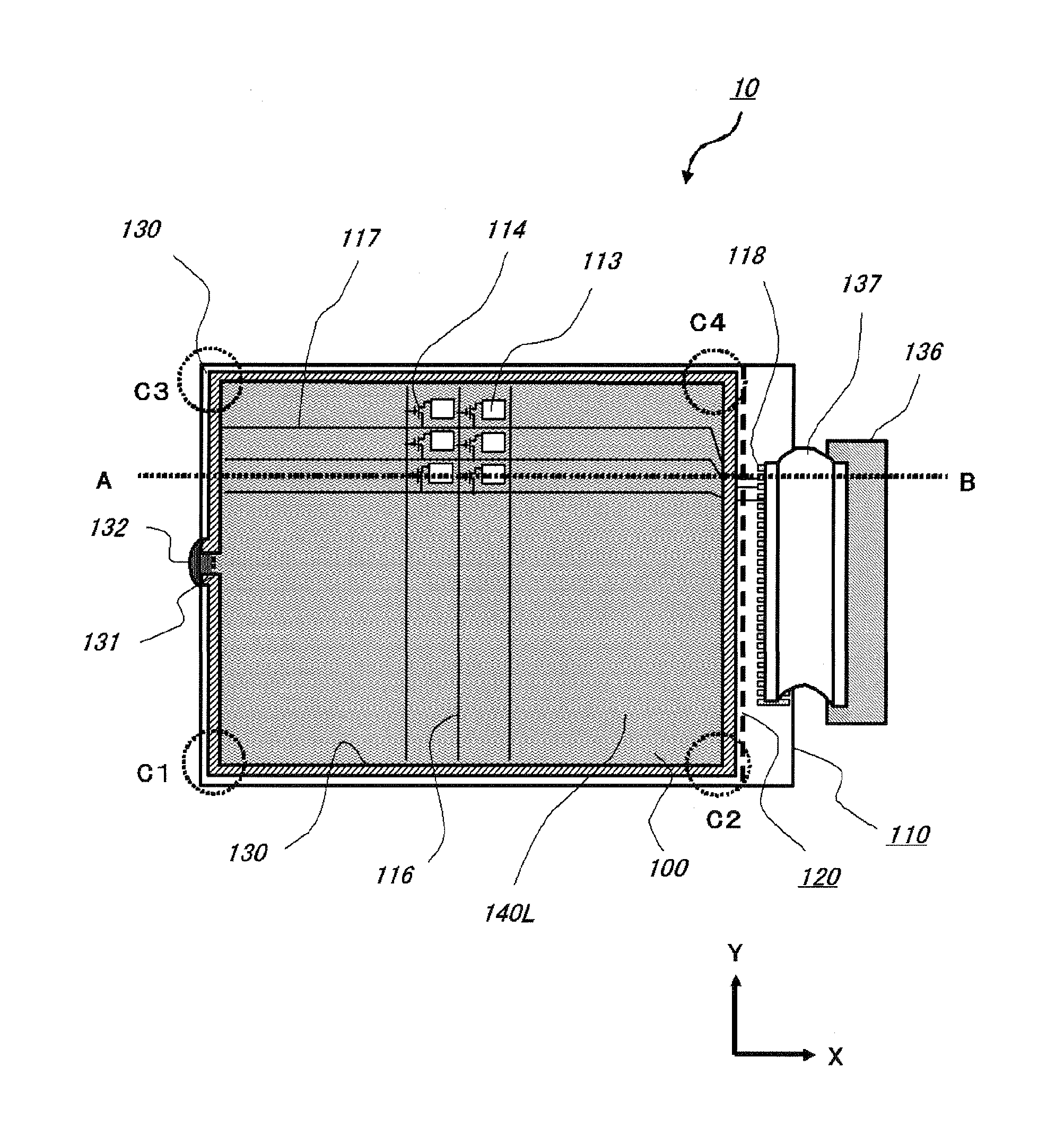
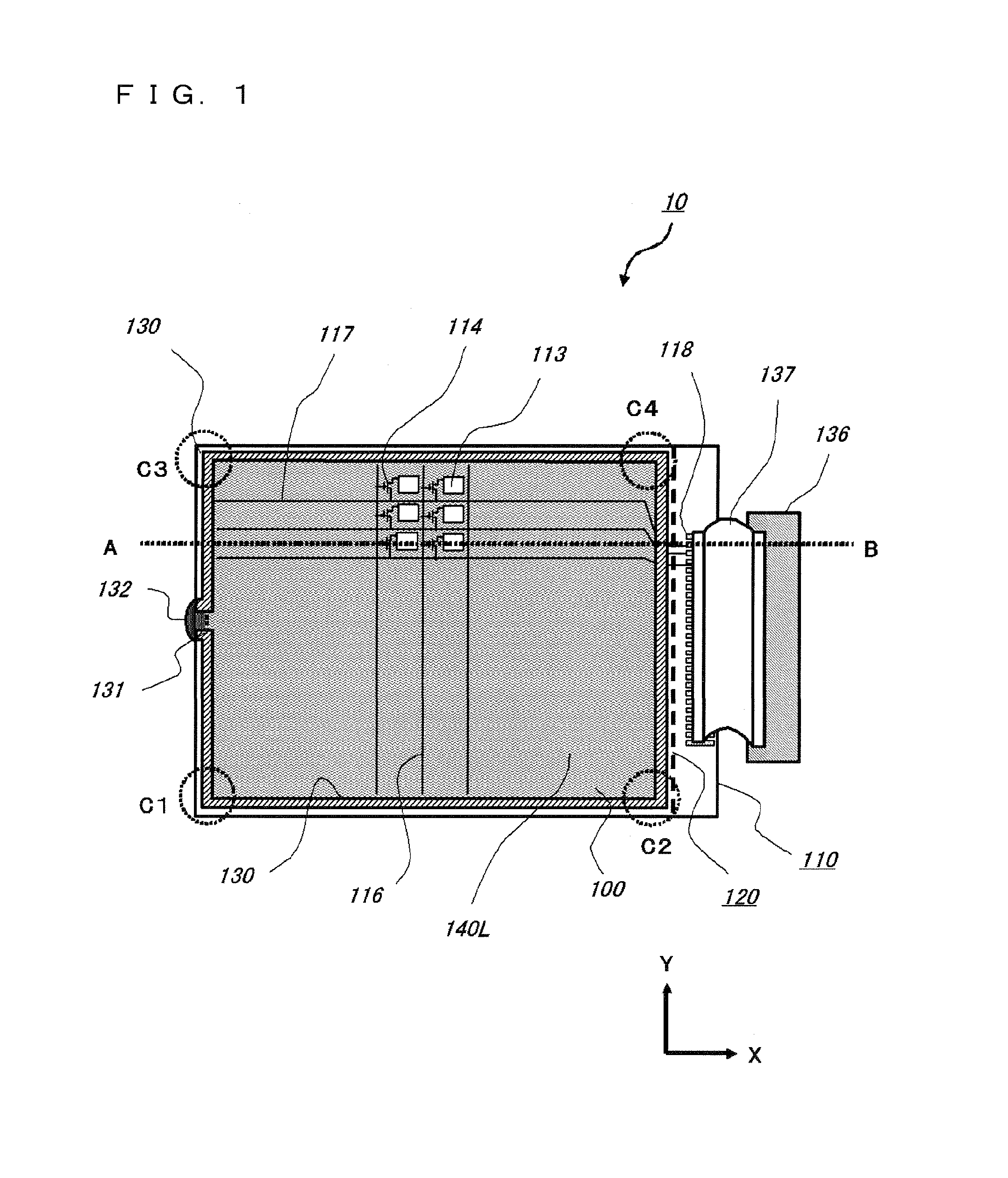
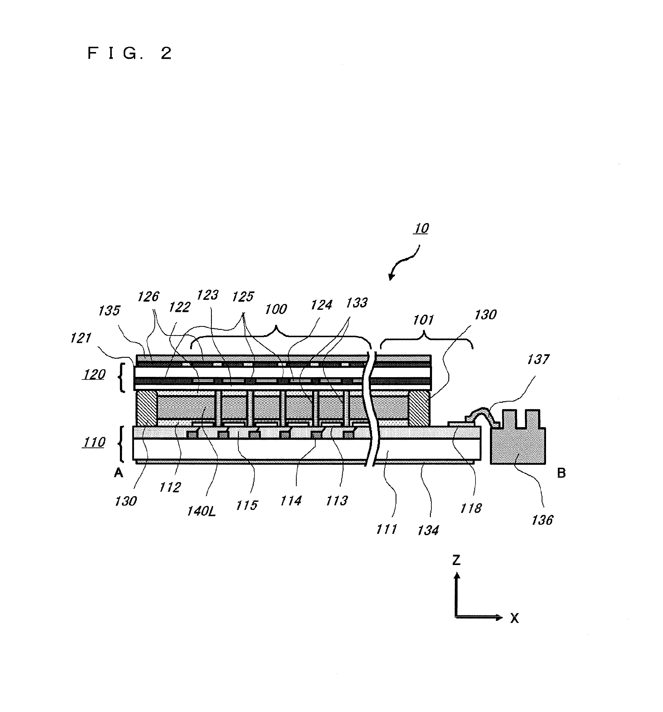
[0029]A configuration of a liquid crystal panel 10 used in a liquid crystal display device according to a preferred embodiment 1 will be described with reference to schematic diagrams of FIGS. 1, 2, 3, and 4. FIG. 1 is a plan view showing a configuration of the whole of a liquid crystal panel. FIG. 2 is a cross-sectional view as taken along the line A-B of FIG. 1. FIGS. 3 and 4 are plan views showing principal area in corner portions C1 and C2 shown in FIG. 1. These drawings are merely schematic, and do not exactly reflect the sizes of component parts, and the like, that are shown therein. To avoid complicating the drawings, as appropriate, parts other than principal parts of the invention are omitted and configurations are partially simplified. The same is true for the subsequent drawings. Moreover, in the subsequent drawings, the same component parts as those illustrated in the already-described drawings are denoted by the same reference numerals, and descrip...


PUM

PropertyMeasurementUnit
thicknessaaaaaaaaaa
thicknessaaaaaaaaaa
thicknessaaaaaaaaaa

Abstract

A liquid crystal display device of the present invention includes a liquid crystal interposed between a CF substrate that is an ultra-thin glass substrate and a TFT substrate, and a seal pattern having an injection port. Spacer structures are arranged such that the area density thereof is higher in a corner portion farther from the injection port than in a corner portion closer to the injection port.

Description

BACKGROUND OF THE INVENTION[0001]1. Field of the Invention[0002]The present invention relates to a liquid crystal display device including ultra-thin glass and a method for manufacturing the liquid crystal display device.[0003]2. Description of the Background Art[0004]In recent years, there has been proposed a liquid crystal display for use in a curved form (curved display) or a liquid crystal display device capable of displaying a dual screen (dual-screen display) in which a parallax barrier is arranged on a display surface of a liquid crystal panel. In these liquid crystal displays, ultra-thin glass is commonly used. For example, Japanese Patent Application Laid-Open No. 2003-337550 mentions a liquid crystal panel including, as ultra-thin glass, a glass substrate having an ultra-thin thickness of about 0.01 to 0.15 mm, in order to achieve a flexibly bendable liquid crystal panel that can be also used in a curved display. Japanese Patent Application Laid-Open No. 2011-128547 disclo...

Claims


Application Information

Patent Timeline
Patent Type & Authority Applications(United States)
IPC IPC(8): G02F1/1339G02B27/22
CPCG02B27/2214G02F1/13394G02B5/201G02F1/1339G02F1/1341G02B30/27G02F1/133302G02F1/13396
Inventor TANIGUCHI, TOSHIROYABIKU, HIDEOFUJINO, TOSHIAKI
Owner TRIVALE TECH LLC
Why Eureka
Try Eureka