Semiconductor device with silicon-containing hard mask and method for fabricating the same

a semiconductor device and hard mask technology, applied in semiconductor devices, capacitors, electrical equipment, etc., can solve the problems of difficult to perform a stable etch process for forming the hard mask pattern, the hard mask pattern having a smaller thickness than the etch target layer may be lost during the etch process, etc., to achieve the effect of preventing bowing and high aspect ratio

Active Publication Date: 2014-02-27
SK HYNIX INC
View PDF2 Cites 16 Cited by
  • Summary
  • Abstract
  • Description
  • Claims
  • Application Information

AI Technical Summary

Benefits of technology

[0006]Exemplary embodiments of the present invention are directed to a semiconductor device and a method for fabricating the same, which is capable of preventing bowing even though the thickness of a hard mask layer increases and forming fine patterns with a high aspect ratio.
[0007]In accordance with an embodiment of the present invention, a semiconductor device includes a semiconductor substrate having an etch target layer provided on the surface thereof, and a hard mask layer formed over the etch target layer and including silicon, wherein the hard mask layer includes a dual structure including a first area and a second area having a larger etch rate than the first area, in order to increase an etching selectivity of the hard mask layer.

Problems solved by technology

This is because, as the aspect ratio increases, the hard mask pattern having a smaller thickness than the etch target layer may be lost during the etch process.
When the aspect ratio of the hard mask pattern increases, it is difficult to perform a stable etch process for forming the hard mask pattern as in the etch process for the etch target layer.

Method used


Image

  • Semiconductor device with silicon-containing hard mask and method for fabricating the same
  • Semiconductor device with silicon-containing hard mask and method for fabricating the same
  • Semiconductor device with silicon-containing hard mask and method for fabricating the same

Examples


first embodiment

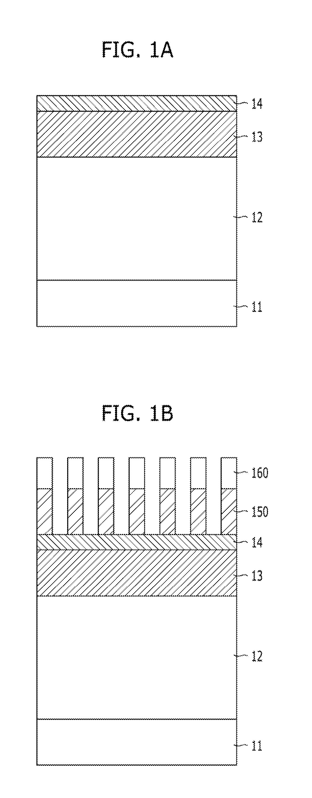
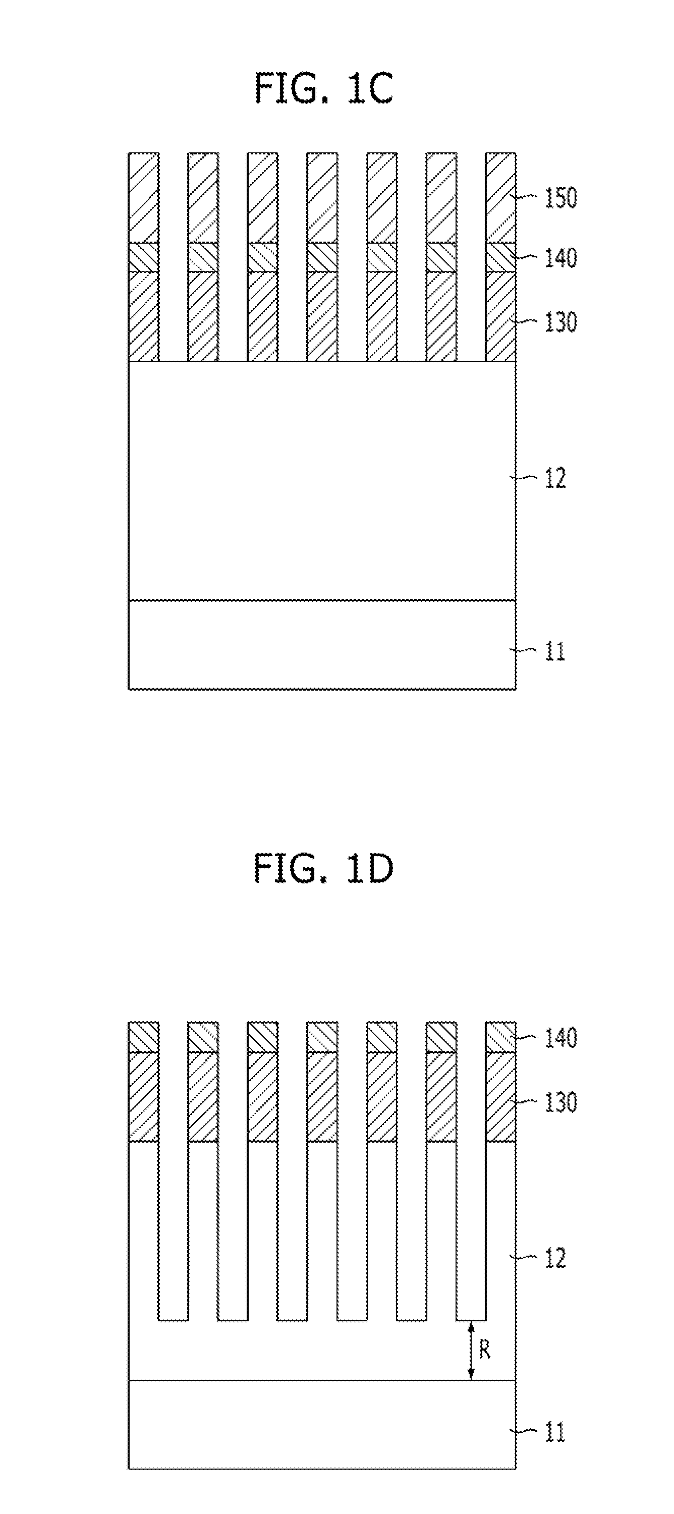
[0014]FIGS. 1A to 1F are diagrams illustrating a method for fabricating a semiconductor device in accordance with the present invention.

[0015]Referring to FIG. 1A, an etch target layer 12 is formed over a semiconductor substrate 11. The etch target layer 12 is a material for forming patterns of a semiconductor device, and may include an insulation layer. For example, the etch target layer 12 may include an oxide layer and a nitride layer. The etch target layer 12 may include a plurality of oxide layers. Alternatively, the etch target layer 12 may include an oxide layer and a nitride layer which are sequentially stacked. Alternatively, the etch target layer 12 may include a plurality of oxide layers and nitride layers that are alternately stacked.

[0016]A hard mask layer is formed over the etch target layer 12. The hard mask layer may include a first area and a second area to increase an etching selectivity. The second area may be formed over the first area, and may have a smaller etc...

second embodiment

[0041]FIGS. 2A to 2H are diagrams illustrating a method for fabricating a semiconductor device in accordance with the present invention.

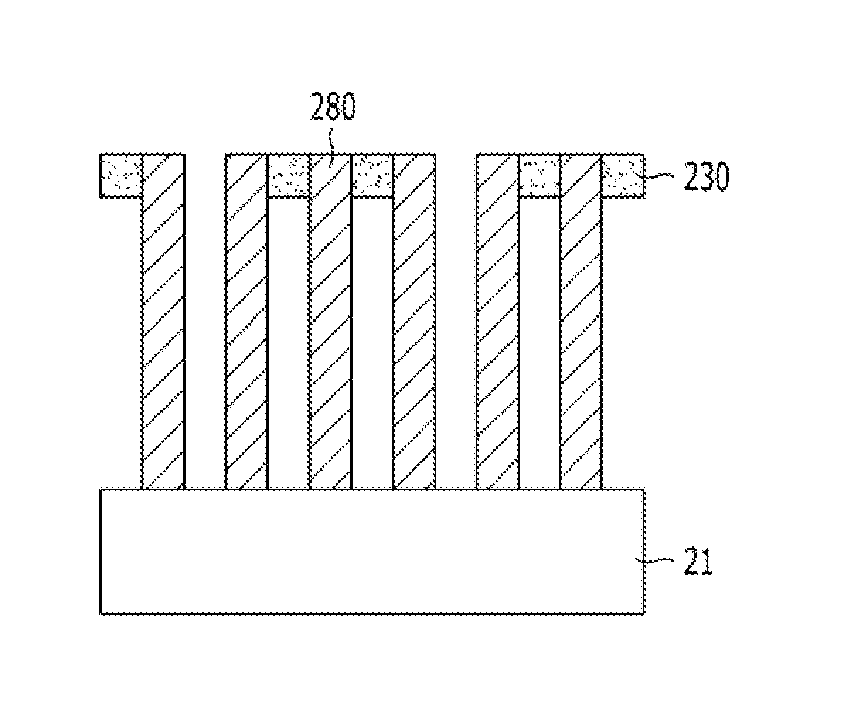
[0042]Referring to FIG. 2A, a mold layer 22 is formed over a semiconductor substrate 21. The mold layer 22 is a material for providing an open space where a storage node of a capacitor is to be formed, and may include an insulation layer. For example, the mold layer 22 may include oxide. The mold layer 22 may include a plurality of oxide layers. The mold layer 22 may have a thickness of about 15,000 Å or more to secure capacitance. Before the mold layer 22 is formed, transistors, bit lines and the like may be formed in the semiconductor substrate. Furthermore, a plug such as a landing plug may be further formed over the semiconductor substrate 21.

[0043]A supporting layer 23 is formed over the mold layer 22. The supporting layer 23 serves to prevent a storage node from collapsing during a wet dip-out process. The supporting layer 23 may include nitri...


PUM

PropertyMeasurementUnit
etch rateaaaaaaaaaa
areaaaaaaaaaaa
doping concentrationaaaaaaaaaa

Abstract

A semiconductor device includes a semiconductor substrate having an etch target layer provided on the surface thereof, and a hard mask layer formed over the etch target layer and including silicon, wherein the hard mask layer includes a dual structure including a first area and a second area having a larger etch rate than the first area, in order to increase an etching selectivity of the hard mask layer.

Description

CROSS-REFERENCE TO RELATED APPLICATIONS[0001]The present application claims priority of Korean Patent Application No. 10-2012-0093045, filed on Aug. 24, 2012, which is incorporated herein by reference in its entirety.BACKGROUND[0002]1. Field[0003]Exemplary embodiments of the present invention relate to a method for fabricating a semiconductor device, and more particularly, to a semiconductor device with a silicon-containing hard mask and a method for fabricating the same.[0004]2. Description of the Related Art[0005]In general, patterns constituting a semiconductor device are formed by forming hard mask patterns over an etch target layer to be patterned and etching the etch target layer exposed between the hard mask patterns. When the hard mask patterns serving as an etch barrier are used to perform the etch process, the etch target layer under the hard mask patterns must not be exposed while the etch target layer exposed between the hard mask patterns is etched. However, as the patt...

Claims


Application Information

Patent Timeline
Patent Type & Authority Applications(United States)
IPC IPC(8): H01L21/308H01L21/311H01L29/06
CPCH01L21/3081H01L21/31144H01L29/06H01L28/90H10B12/033H01L21/02123H01L21/02129H01L21/0337H01L21/32055
Inventor LEE, SUNG-KWONSUN, JUN-HYEUBJUNG, YOUNG-KYUN
Owner SK HYNIX INC
Why Eureka
Try Eureka