Ion sensitive field effect transistor

a field effect transistor and sensitive technology, applied in the direction of material analysis by electric/magnetic means, measurement devices, instruments, etc., can solve the problems of increasing the noise in the readout, relative high manufacturing costs, etc., and achieves low noise, relatively fast operation, and high-performance ion detection

Active Publication Date: 2014-03-06
X FAB SEMICON FOUNDRIES
View PDF5 Cites 15 Cited by
  • Summary
  • Abstract
  • Description
  • Claims
  • Application Information

AI Technical Summary

Benefits of technology

[0014]Advantageously, the integrated CMOS or bipolar process can be optimized such that the ISFET provides high performance ion detection. The CMOS or bipolar based ISFET according to embodiments of the invention enables the ion sensitive recess and signal readout circuit to be integrated within a single chip. Since the signal transmission and processing are performed on the same chip, these operations are relatively fast and produce less noise than the conventional ISFET. As a result, the signal readout or sensitivity of the ISFET is improved. The improvement in the signal readout or sensitivity of the ISFET is particularly noticeable if the ion sensitive recess is fabricated directly on top of the gate of the ISFET. The utilization of the standard CMOS process may also result in low manufacturing cost. Furthermore, the invention enables the ISFET fabrication in arrays. Therefore, the on-die analysis of a biological reaction and ion concentration becomes easier and cheaper.

Problems solved by technology

The present inventors have found that the above conventional technique may result in relatively high manufacturing costs and increased noise in the readout.

Method used


Image

  • Ion sensitive field effect transistor
  • Ion sensitive field effect transistor
  • Ion sensitive field effect transistor

Examples


first embodiment

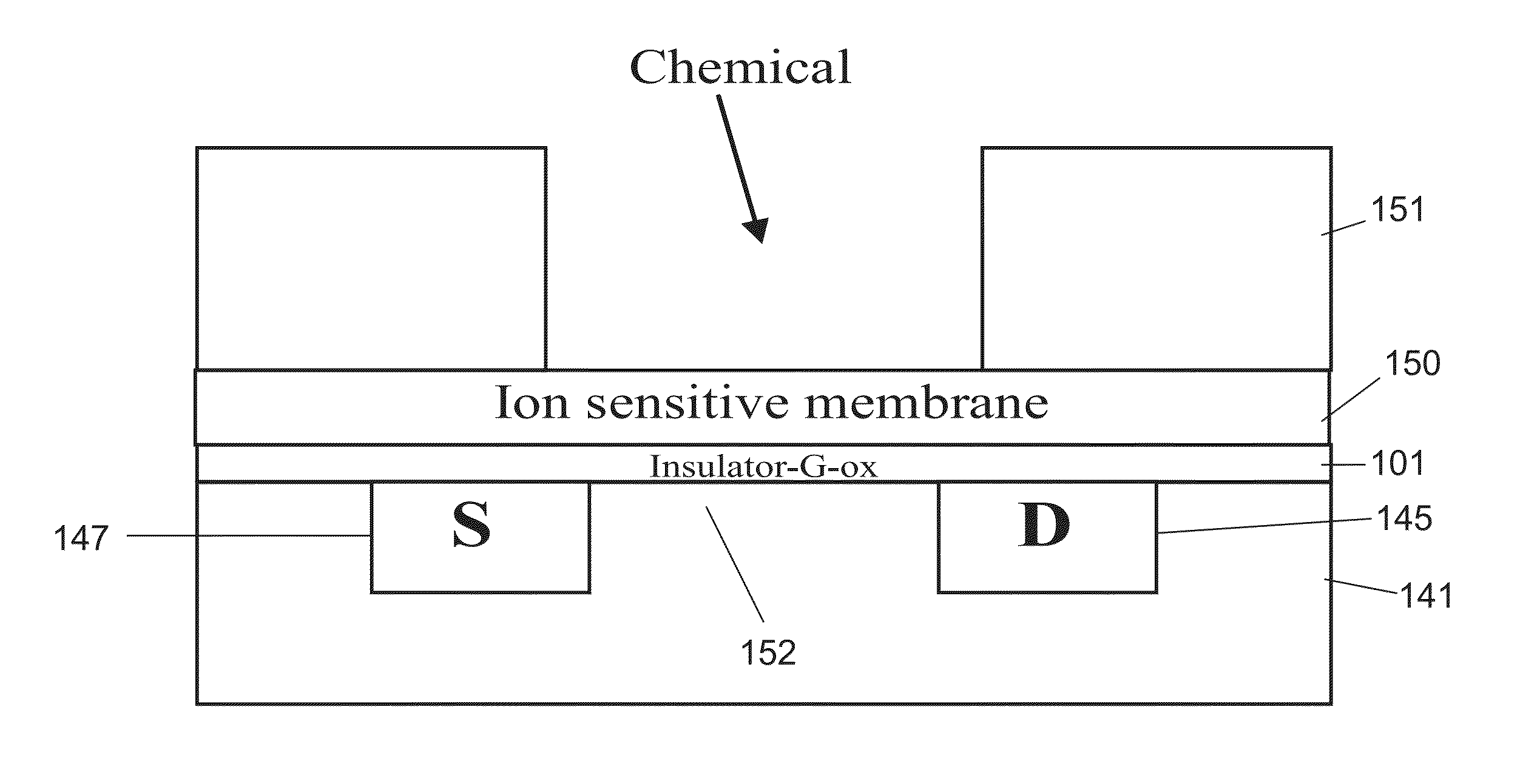
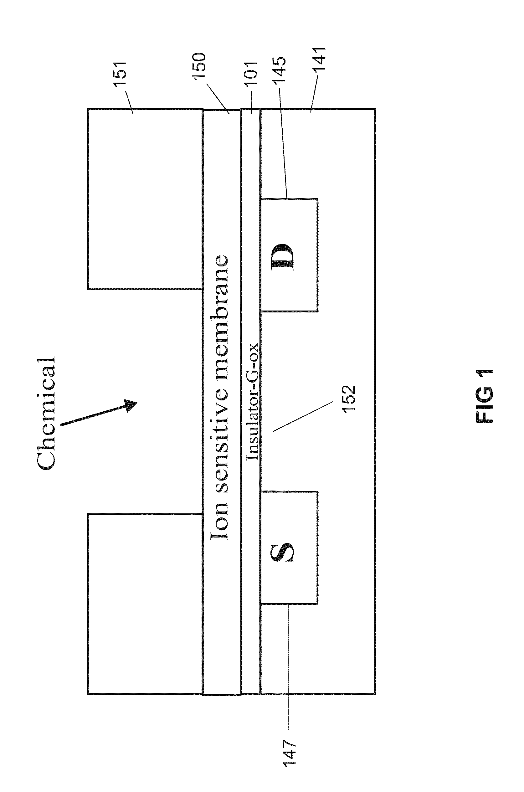
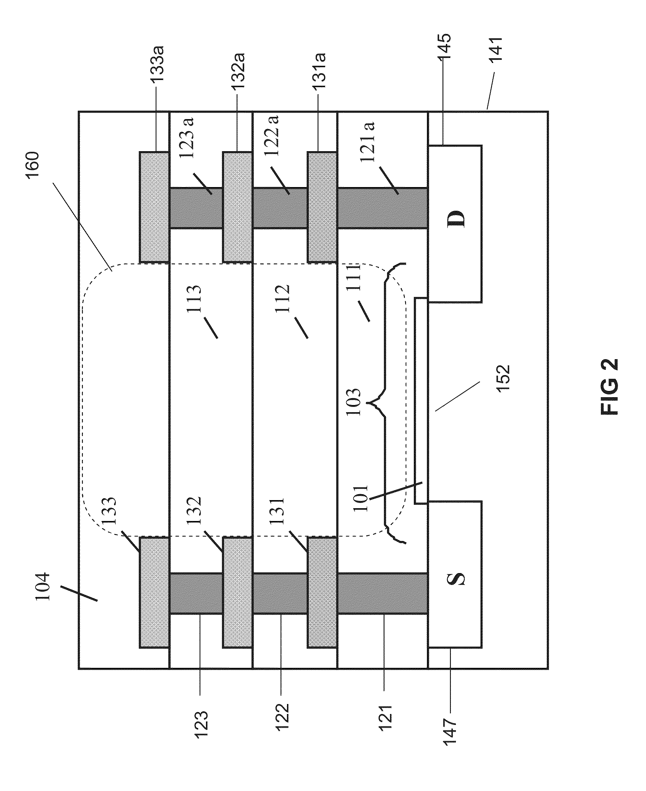
[0026]FIG. 2 is a schematic cross section of an ISFET at one stage of the fabrication according to the present invention. A basic CMOS device is provided comprising a semiconductor substrate 141 having a source 147, a drain 145 and a channel region 152 between the source 147 and the drain 145. A gate consisting of an insulator 101 is located on top of the channel region 152. In certain embodiments, the thickness of the insulator is not less than about 5 nm and is not more than about 150 nm. The thickness of the insulator is preferably about 50 nm or 55 nm. The device also comprises inter-layer dielectric (ILD) 111 covering the insulator 101 and the substrate 141. Inter-metal dielectrics (IMD) 112, 113 are provided on top of the ILD 111. Inter metals 131 and 131a are provided on top of the ILD 111 within IMD 112. Inter metal 131 is connected with the source 147 by contact plug 121, and inter metal 131a is connected with the drain 145 by contact plug 121a. Further inter metals 132, 13...

second embodiment

[0032]FIG. 5 is a schematic cross section of an ISFET at one stage of the fabrication according to the present invention. All the features of the CMOS device of FIG. 5 are similar to those of the CMOS device of FIG. 2, except that an additional poly gate 102 is provided on top of the insulator 101.

[0033]FIG. 6 is a schematic cross section of an ISFET at a second stage of the fabrication according to the second embodiment of the present invention. The fabrication steps for this embodiment are the same as those described in relation to FIG. 3, except that the etching of the dielectric area 103 (of FIG. 5) is carried out down to the surface of the poly gate 102.

[0034]FIG. 7 is a schematic cross section of an ISFET at a third stage of the fabrication according to the second embodiment of the present invention. The fabrication steps for this embodiment are also the same as those described in relation to FIG. 4, except that the ion sensitive membrane 105 is deposited over the entire reces...


PUM

PropertyMeasurementUnit
contact areaaaaaaaaaaa
thicknessaaaaaaaaaa

Abstract

A CMOS or bipolar based Ion Sensitive Field Effect Transistor (ISFET) comprising an ion sensitive recess for holding a liquid wherein the recess is formed at least partly on top of a gate of the transistor. There is also provided a method of manufacturing an I on Sensitive Field Effect Transistor (ISFET) utilizing CMOS processing steps, the method comprising forming an ion sensitive recess for holding a liquid at least partly on top of a gate of the transistor.

Description

CROSS REFERENCE TO RELATED APPLICATIONS[0001]This application is a continuation of International Patent Application Number PCT / EP2011 / 057359 filed on 6 May 2011, the contents of which are herein incorporated by reference in their entirety.TECHNICAL FIELD[0002]The present invention relates to an Ion Sensitive Field Effect Transistor (ISFET), and in particular to an ISFET manufactured utilizing CMOS or bipolar processing steps.BACKGROUND[0003]Electronic devices and components have found numerous applications in measurement and monitoring of chemical or biological reactions such as detecting concentration, presence and activity of particular ions, enzymes, antibodies, antigens, hormones and gases. One such electronic device is referred to as an Ion Sensitive Field Effect Transistor, often denoted in the relevant literature as ISFET. This device facilitates the measurement, for example, of a hydrogen ion concentration (i.e. pH) in a solution.[0004]FIG. 1 is a schematic cross-section of ...

Claims


Application Information

Patent Timeline
Patent Type & Authority Applications(United States)
IPC IPC(8): G01N27/414
CPCG01N27/414G01N27/4148
Inventor KOO, SANG SOOLFANG, LING GANG
Owner X FAB SEMICON FOUNDRIES
Why Eureka
Try Eureka