Interfacial alloy layer for improving electromigration (EM) resistance in solder joints

a technology of interfacial alloy and solder joints, which is applied in the direction of welding/cutting media/materials, manufacturing tools, and soldering apparatus, etc., can solve the problems of increasing electromigration (em) resistance, device completely inoperable, and portion of the circuit becoming disconnected, etc., to achieve the effect of improving electromigration (em) resistance in solder joints

Active Publication Date: 2014-03-06
IBM CORP
View PDF2 Cites 15 Cited by
  • Summary
  • Abstract
  • Description
  • Claims
  • Application Information

AI Technical Summary

Benefits of technology

[0031]The present invention is able to improve electromigration (EM) resistance in solder joints.

Problems solved by technology

In addition, there is demand for more reliable semiconductor packages and, as integrated circuits become increasingly miniaturized, electromigration (EM) resistance has become a growing issue and its effects can no longer be ignored.
In the worst case, a portion of the circuit becomes disconnected, and the device rendered completely inoperable.
However, electromigration remains a problem in joints between semiconductor chips and package substrates as the power consumed per unit area of conductor increases because the current density in these joints is higher.
However, when current is applied for a long period of time, voids caused by electromigration occur, and resistance increases.
Moreover, even when copper is used, there are still some effects of electromigration.
However, a defect called a black pad sometimes occurs on the organic substrate side.
If a Ni barrier is simply used on the chip side, the copper in the pad on the organic substrate side moves (elutes) into the solder, and this has adverse effects such as a rise in resistance.
However, Patent Literature 2 and Patent Literature 3 require special solder balls and insulating layers, neither of which will remain viable as the joint pitches of semiconductor chips are further miniaturized.

Method used


Image

  • Interfacial alloy layer for improving electromigration (EM) resistance in solder joints
  • Interfacial alloy layer for improving electromigration (EM) resistance in solder joints
  • Interfacial alloy layer for improving electromigration (EM) resistance in solder joints

Examples


Embodiment Construction

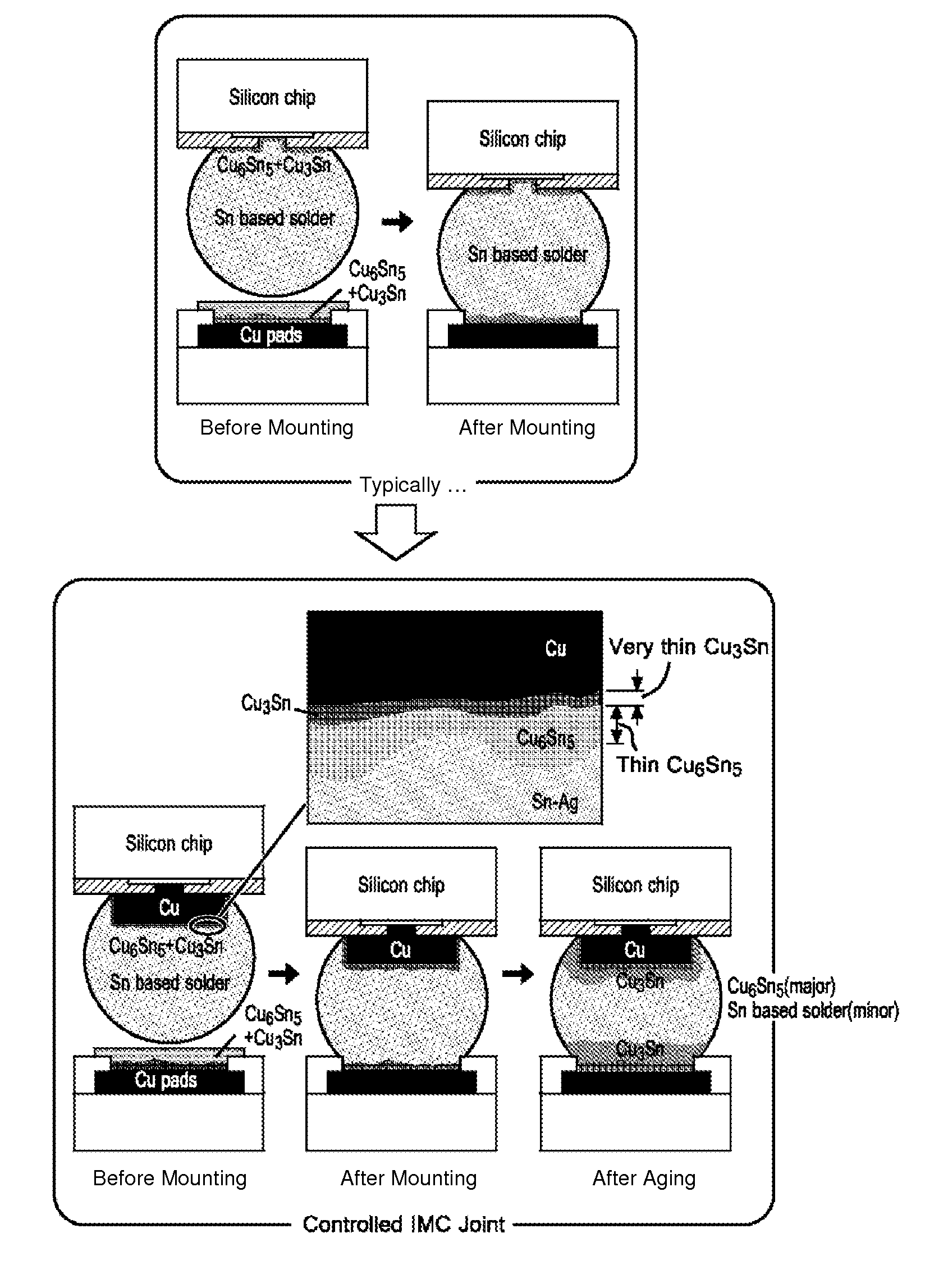
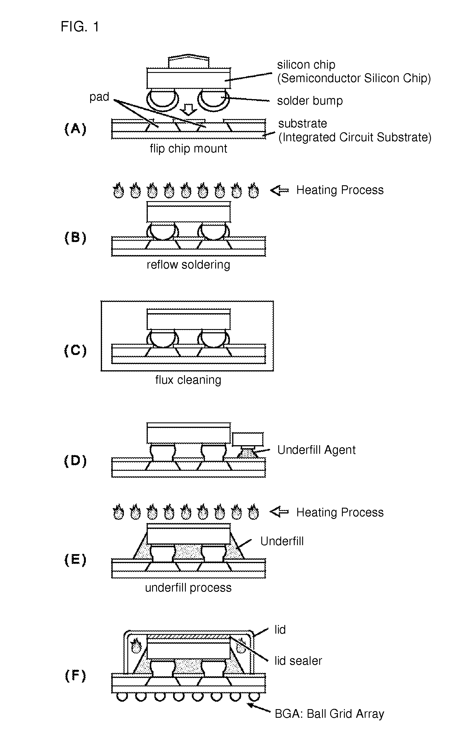
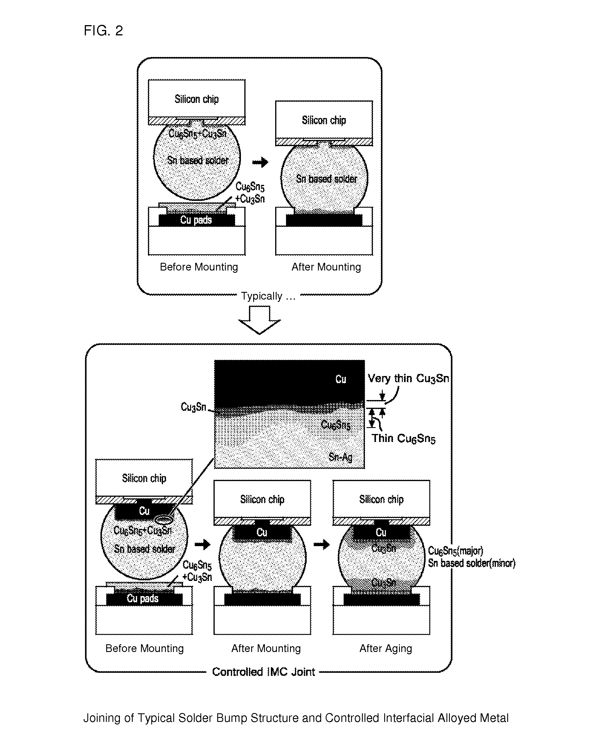
[0040]FIG. 1 is a diagram used to explain the configuration of a typical semiconductor package, and a method for manufacturing this package.

[0041]In the manufacture of a semiconductor package with multiple terminals, flip chips, including the C4 method, have gradually been adopted as the mounting method in place of conventional wire bonding.

[0042]The C4 method is an abbreviation for the controlled collapse chip connection method. Here, the expression C4 is derived from the first letter “C” in each of the four words.

[0043]Hump-shaped conductive protrusions called bumps are formed on the electrodes of a wafer for bonding to a substrate.

[0044]The use of this method makes a reduced mounting area and a smaller product possible. Because the wiring in the semiconductor is also shorter, the electrical characteristics are improved.

[0045]First, as shown in FIG. 1 (A), hump-shaped conductive protrusions called solder bumps are formed on a silicon chip (semiconductor silicon chip).

[0046]A solde...


PUM

PropertyMeasurementUnit
thicknessaaaaaaaaaa
temperatureaaaaaaaaaa
diameteraaaaaaaaaa

Abstract

Problem
To improve the electromigration (EM) resistance of a solder joint.
Solution
The present invention provides a unique structure for an interfacial alloy layer which is able to improve the electromigration (EM) resistance of a solder joint, and a unique method of forming this structure. More specifically, in this unique structure, a controlled interfacial alloy layer is provided on both sides of a solder joint. In order to form this structure, aging (maintenance of high-temperature conditions) is performed until an interfacial alloy layer of Cu3Sn has a thickness of at least 1.5 μm.

Description

TECHNICAL FIELD[0001]The present invention relates generally to a semiconductor package and to a manufacturing method therefor. The present invention relates more specifically to a unique structure for an interfacial alloy layer which is able to improve the electromigration (EM) resistance of a solder joint, and a unique method of forming this structure.BACKGROUND ART[0002]With the demand for smaller and lighter electronic devices, it is expected to realize more highly integrated semiconductor packages.[0003]In addition, there is demand for more reliable semiconductor packages and, as integrated circuits become increasingly miniaturized, electromigration (EM) resistance has become a growing issue and its effects can no longer be ignored.[0004]Electromigration (EM) is a phenomenon in which there is a momentum exchange between electrons moving through an electrical conductor and metal atoms, the metal atoms gradually move, and defects (voids) occur in the shape of the metal. This phen...

Claims


Application Information

Patent Timeline
Patent Type & Authority Applications(United States)
IPC IPC(8): H01L23/00
CPCH01L24/03H01L24/08H01L24/81H01L21/50H01L21/563H01L24/05H01L24/11H01L24/13H01L24/16H01L24/29H01L24/32H01L24/33H01L24/83H01L24/92H01L2224/03828H01L2224/0401H01L2224/05147H01L2224/05647H01L2224/11849H01L2224/13026H01L2224/131H01L2224/13111H01L2224/16225H01L2224/16227H01L2224/16503H01L2224/2919H01L2224/32225H01L2224/33181H01L2224/73204H01L2224/73253H01L2224/81191H01L2224/81192H01L2224/81193H01L2224/81447H01L2224/81815H01L2224/8191H01L2224/81948H01L2224/83102H01L2224/83862H01L2224/92H01L2224/92125H01L2224/92225H01L2924/01327H01L2924/014H01L2924/10253H01L2924/15153H01L2924/15311H01L2924/16152H01L2924/20105H01L2924/3512H01L2924/3656
Inventor NOMA, HIROKAZUORII, YASUMITSUTORIYAMA, KAZUSHIGE
Owner IBM CORP
Why Eureka
Try Eureka