

Filtering device with slotted ground structure
- Summary
- Abstract
- Description
- Claims
- Application Information
AI Technical Summary
Benefits of technology
Problems solved by technology
Method used
Image

Examples
Embodiment Construction
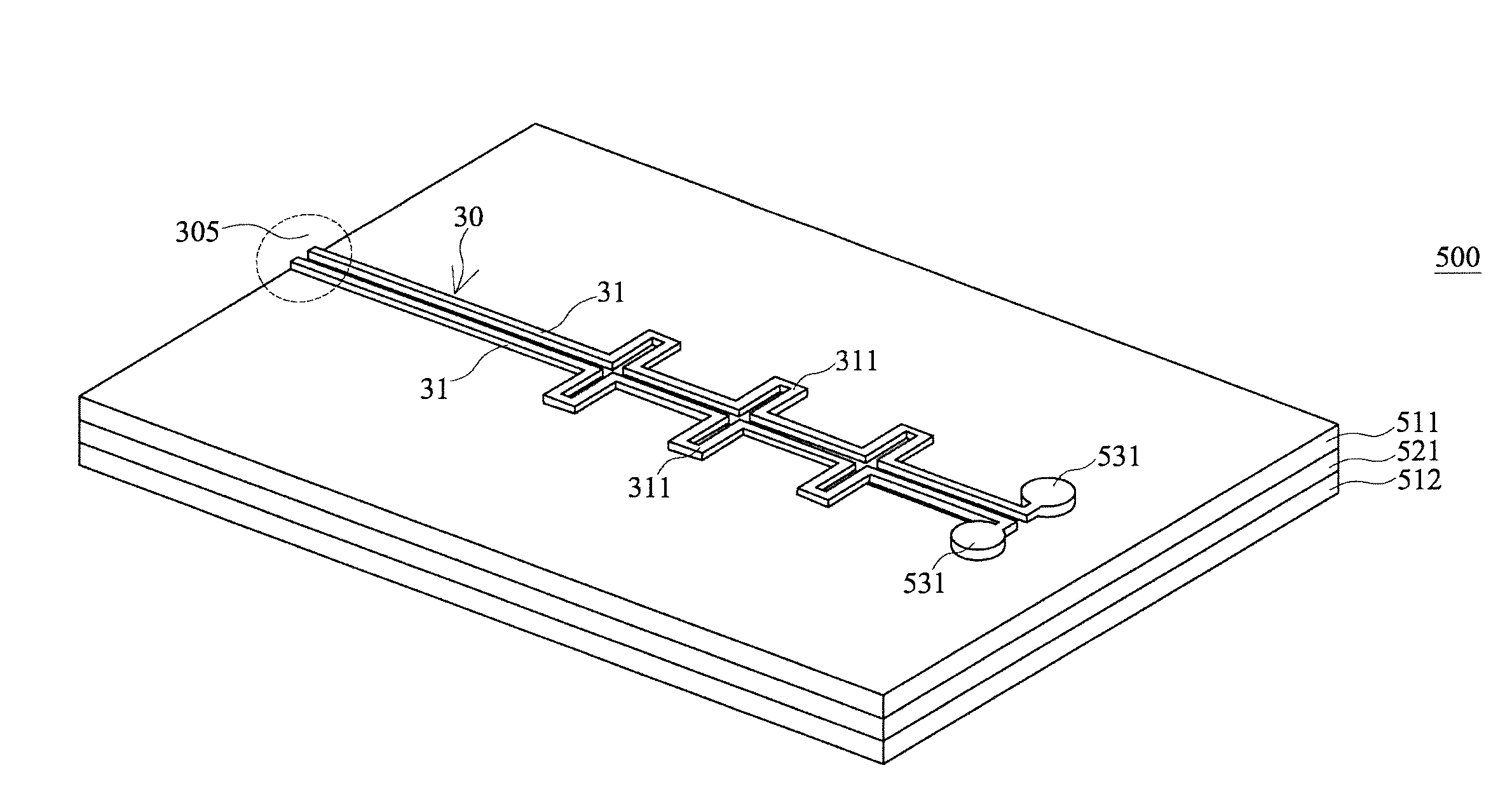
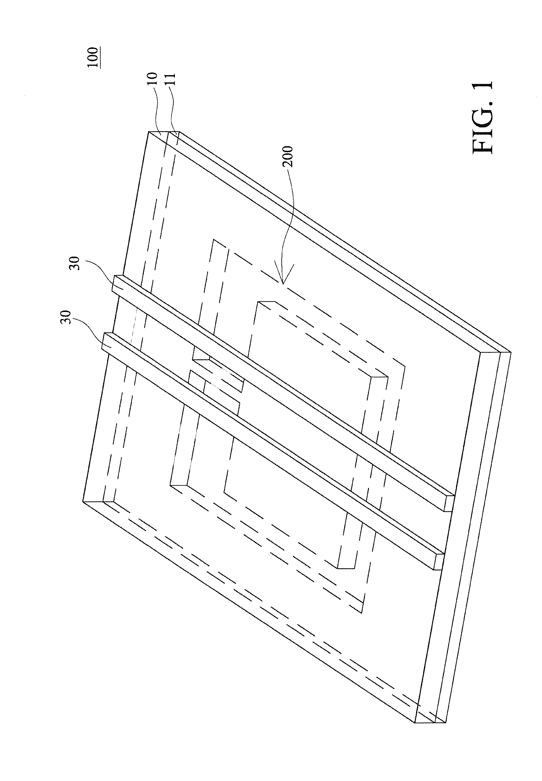
[0049]Referring to FIG. 1, there is shown a three-dimensional structural view of a filtering device with slotted ground structure according to one preferred embodiment of the present invention. As illustrated in the figure, the filtering device 100 comprises a substrate 10, a ground plane 11 and a pair of differential signal lines 30.
[0050]In this case, two differential signal lines 30 are provided on the top surface of the substrate 10 in parallel and symmetrically with respect to each other in the form of a micro strip line, an embedded micro strip line or a strip line. Moreover, an electromagnetic coupling is generated between the two signal lines 30.
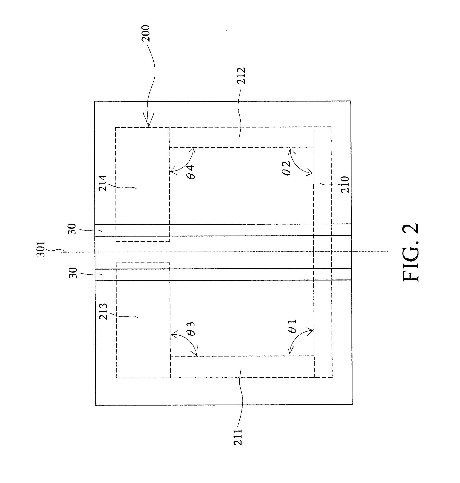
[0051]The ground plane 11 is provided on the bottom surface of the substrate 10 and is a metal joining of the substrate 10. Furthermore, the ground plane 11 is etched to be different shapes so as to obtain a slotted ground structure 200. In practical differential transmission, one differential-mode signal and one common-mode noise ar...
PUM
 Abstract
Description
Claims
Application Information