Substrate processing apparatus and substrate processing method

a processing apparatus and substrate technology, applied in the direction of liquid surface applicators, pretreated surfaces, coatings, etc., can solve the problems of defective dimension, defective shape of exposure pattern, contamination of substrate edges, etc., and achieve the effect of preventing the processing of substrate defects due to contamination at the edge of the substra

Active Publication Date: 2014-03-06
SCREEN SEMICON SOLUTIONS CO LTD
View PDF4 Cites 9 Cited by
  • Summary
  • Abstract
  • Description
  • Claims
  • Application Information

AI Technical Summary

Benefits of technology

[0045]In this manner, the first, second and third holders do not come into contact with the edge of the substrate during transportation of the substrate, during supply of the processing liquid to the one surface of the substrate by the one or plurality of processing liquid supply units and during the temperature processing for the substrate by the temperature processing unit. Thus, a contaminant that occurs when a member for holding the substrate comes into contact with the edge of the substrate is prevented. Further, a contaminant is prevented from being transferred from the first, second and third holders to the edge of the substrate. As a result, a processing defect of the substrate due to contamination at the edge of the substrate is prevented.

Problems solved by technology

Although the substrate is subjected to various types of film formation processing before the exposure processing, an edge of the substrate may, in some cases, be contaminated in the process of the film formation processing.
When the substrate is subjected to the exposure processing with the edge of the substrate thus contaminated, a defective dimension and a defective shape of an exposure pattern may occur.

Method used


Image

  • Substrate processing apparatus and substrate processing method
  • Substrate processing apparatus and substrate processing method
  • Substrate processing apparatus and substrate processing method

Examples


Embodiment Construction

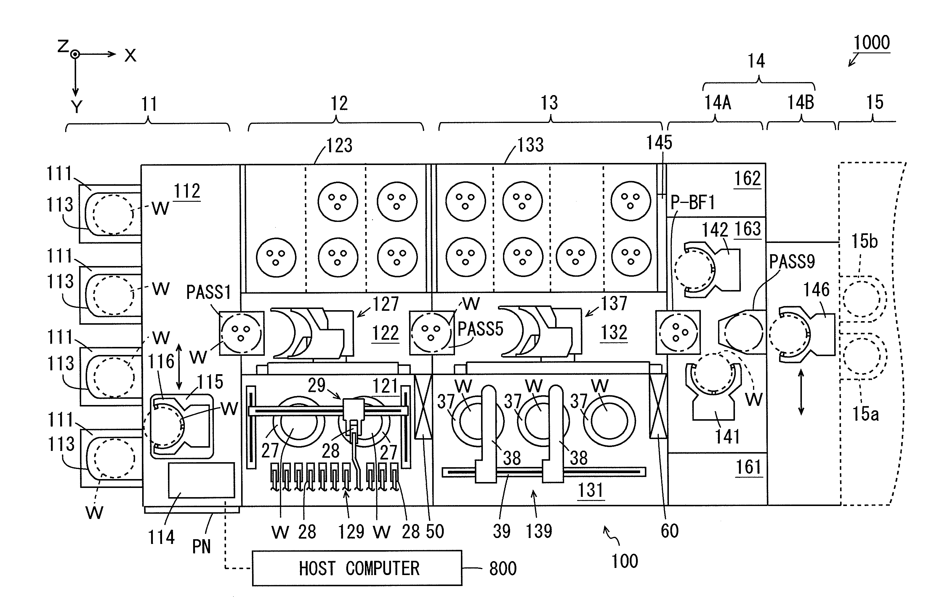
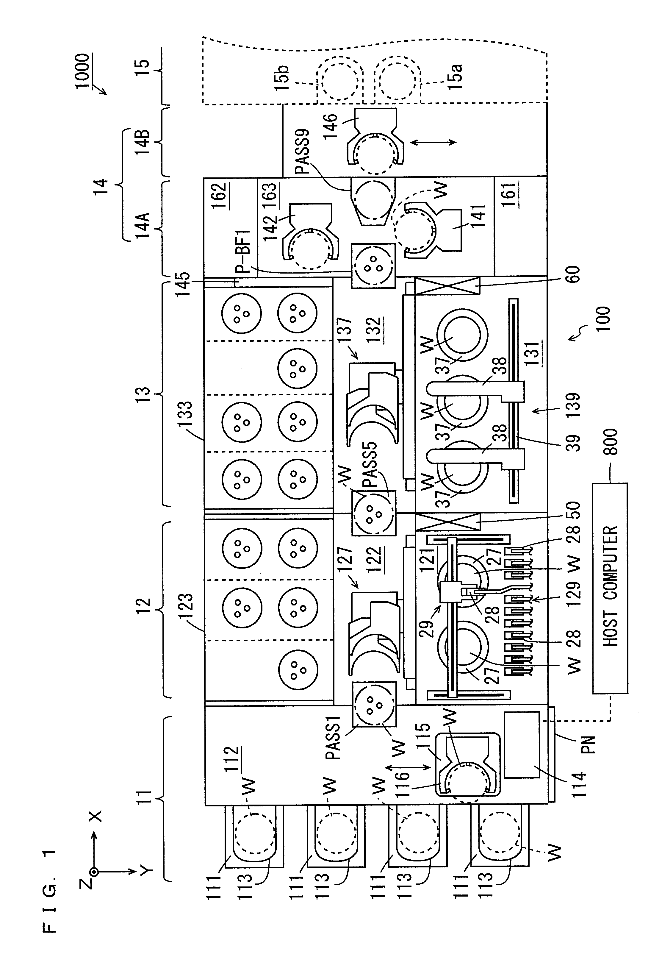
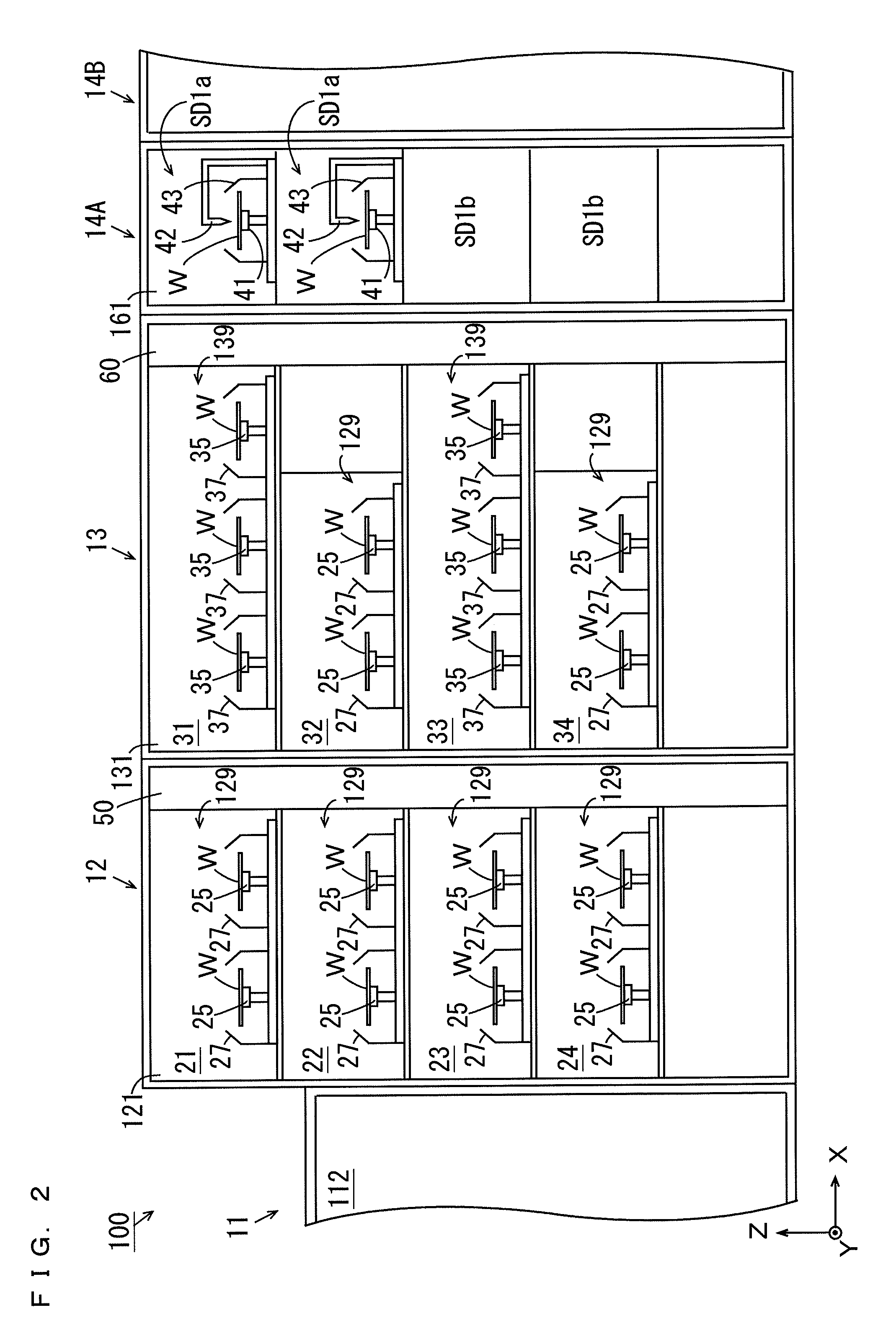
[0081]A substrate processing apparatus and a substrate processing method according to one embodiment of the invention will be described with reference to the drawings. In the following description, a substrate refers to a semiconductor substrate, a substrate for a liquid crystal display, a substrate for a plasma display, a glass substrate for a photomask, a substrate for an optical disk, a substrate for a magnetic disk, a substrate for a magneto-optical disk, a substrate for a photomask and the like.

[0082](1) Configuration of Substrate Processing System

[0083]FIG. 1 is a schematic plan view of a substrate processing system according to the one embodiment of the present invention. FIGS. 1 and subsequent given diagrams are accompanied by the arrows that indicate X, Y, and Z directions orthogonal to one another for clarity of a positional relationship. The X and Y directions are orthogonal to each other within a horizontal plane and the Z direction corresponds to a vertical direction. I...


PUM

PropertyMeasurementUnit
angleaaaaaaaaaa
temperatureaaaaaaaaaa
photosensitiveaaaaaaaaaa

Abstract

Transport mechanisms are respectively provided in first and second processing blocks. Each transport mechanism has a hand. The hand holds the other surface of a substrate without coming into contact with an edge of the substrate. The hand is moved such that the substrate is transported between an adhesion reinforcement processing unit or a cooling unit and a coating processing unit or a development processing unit. In the adhesion reinforcement processing unit and the cooling unit, temperature processing is performed on the substrate while the back surface of the substrate is held by suction. In the coating processing unit and the development processing unit, a processing liquid is supplied to the main surface of the substrate while the back surface of the substrate is held by suction by a spin chuck.

Description

BACKGROUND OF THE INVENTION[0001]1. Field of the Invention[0002]The present invention relates to a substrate processing apparatus and a substrate processing method for performing predetermined processing on a substrate.[0003]2. Description of Related Art[0004]A substrate processing apparatus is used to apply a variety of processing to substrates such as semiconductor substrates, substrates for use in liquid crystal displays, plasma displays, optical discs, magnetic discs, magneto-optical discs, photomasks, and other substrates.[0005]Such a substrate processing apparatus generally subjects a single substrate to a plurality of different types of processing successively. The substrate processing apparatus as described in JP 2003-324139 A is constituted by an indexer block, an anti-reflection film processing block, a resist film processing block, a development processing block, and an interface block. An exposure device that is an external device separated from the substrate processing ...

Claims


Application Information

Patent Timeline
Patent Type & Authority Applications(United States)
IPC IPC(8): G03F7/16
CPCG03F7/16H01L21/67028H01L21/67046H01L21/6838
Inventor KASHIYAMA, MASAHITONISHIYAMA, KOJI
Owner SCREEN SEMICON SOLUTIONS CO LTD
Why Eureka
Try Eureka