Solid-state imaging device

a solid-state imaging and imaging device technology, applied in the direction of diodes, semiconductor devices, radiation control devices, etc., can solve problems such as dark current, and achieve the effect of stabilizing the stable electric potential of the well region

Active Publication Date: 2014-04-03
PANASONIC INTELLECTUAL PROPERTY MANAGEMENT CO LTD
View PDF8 Cites 12 Cited by
  • Summary
  • Abstract
  • Description
  • Claims
  • Application Information

AI Technical Summary

Benefits of technology

[0013]According to the solid-state imaging device pertaining to the present disclosure, the electric potential of the well region is stable, because the well region is connected to the substrate, which is maintained at a fixed electric potential, via the connection region. Also, since the connection region is not formed on the regions where the gates of the transistors are to be formed or the well region where the photoelectric converter is to be formed, but are formed between the well region and the substrate. Therefore, the connection region does not limit the regions for the photoelectric converter and the transistors.
[0014]Thus, the solid-state imaging device pertaining to the present disclosure is capable of stabilizing the electric potential of the well region without limiting the regions for forming the photoelectric converter and the transistors.

Problems solved by technology

There is another problem that electrical charge generated in the well region 910 due to thermal excitation could cause dark current.

Method used


Image

  • Solid-state imaging device
  • Solid-state imaging device
  • Solid-state imaging device

Examples


embodiment 1

1. Structure of Solid-State Imaging Device 100

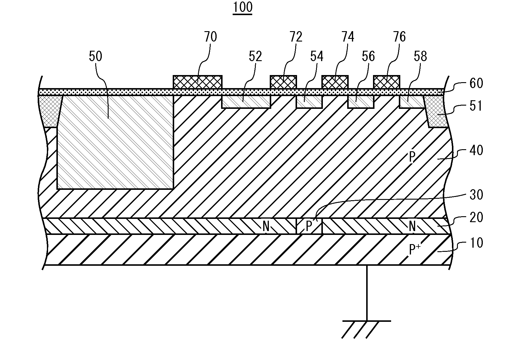
[0031]FIG. 1A is a cross-sectional view of a solid-state imaging device 100 pertaining to Embodiment 1 of the present disclosure, and FIG. 1B is a layout diagram showing a modification example of the positional relationship between transistors and a connection region. Note that the cross section along the line A-A shown in the plan view of the solid-state imaging device 100 shown in FIG. 1B corresponds to FIG. 1A.

[0032]As shown in FIG. 1A, the solid-state imaging device 100 includes: a P+-type (first conductivity type with a high concentration of impurities) silicon substrate 10; an N-type (second conductivity type) dark-current drain region 20 formed on the silicon substrate 10; a P-type (first conductivity type) connection region 30 formed on the region within the silicon substrate 10 where the dark-current drain region 20 are not formed; a P-type (first conductivity type) well region 40 formed over the dark-current drain region 20 and...

embodiment 2

1. Structure of Solid-State Imaging Device 200

[0054]FIG. 5A is a cross-sectional view of a solid-state imaging device 200 pertaining to Embodiment 2 of the present disclosure, and FIG. 5B is a layout diagram showing the positional relationship between the transistors and the connection region. The solid-state imaging device 200 has the same elements as the solid-state imaging device 100 except for the elements described below, and explanation of the same elements is therefore omitted.

[0055]As shown in FIG. 5A, the solid-state imaging device 200 includes a dark-current drain region 220 composed of a first dark-current drain region 222 and a second dark-current drain region 224. The section corresponding in position to the photodiode 50 includes the first dark-current drain region 222, but does not include the second dark-current drain region 224. The top surface of the first dark-current drain region 222 is at a greater depth than the bottom surface of the photodiode 50, and the top ...

embodiment 3

1. Structure of Solid-State Imaging Device 300

[0061]FIG. 7A is a cross-sectional view of a solid-state imaging device 300 pertaining to Embodiment 3 of the present disclosure, and FIG. 7B is a layout diagram showing the positional relationship between transistors and a connection region. The solid-state imaging device 300 has the same elements as the solid-state imaging device 100 except for the elements described below, and explanation of the same elements is therefore omitted.

[0062]As shown in FIG. 7A, the solid-state imaging device 300 includes: an insulating film 90 which is formed to cover the gate oxide film 60 and in which a connection layer 92 is embedded, the connection layer being composed of a contact region, a plurality of metal wiring lines, and a via; a lower electrode 94 formed on the insulating film 90, a photoelectric conversion film 96 spreading to cover the lower electrode 94; and an upper electrode 98 made of light-transmissive conductive material and covering th...


PUM

PropertyMeasurementUnit
distanceaaaaaaaaaa
distanceaaaaaaaaaa
electric potentialaaaaaaaaaa

Abstract

A solid-state imaging device including: a semiconductor substrate of a first conductivity type, having a fixed electric potential; a dark-current drain region of a second conductivity type, formed on a portion of the semiconductor substrate; a connection region of the first conductivity type, formed on another portion of the semiconductor substrate where the dark-current drain region is not formed; a well region of the first conductivity type, covering the dark-current drain region and the connection region; and a first region and a second region, formed within the well region and constituting a part of a read transistor that reads signal charge generated by photoelectric conversion. The well region is maintained at a fixed electric potential by being connected to the semiconductor substrate via the connection region.

Description

CROSS REFERENCE TO RELATED APPLICATION[0001]This is a continuation application of PCT Application No. PCT / JP2012 / 004029 filed Jun. 21, 2012, designating the United States of America, the disclosure of which, including the specification, drawings and claims, is incorporated herein by reference in its entirety.TECHNICAL FIELD[0002]The present disclosure relates to a solid-state imaging device, and in particular to a technology of fixing the electric potential of a well region.BACKGROUND ART[0003]A solid-state imaging device 900 shown in FIG. 16 is an example of conventional solid-state imaging devices. The solid-state imaging device 900 has a pixel region where pixels are two-dimensionally arrayed, and a peripheral region surrounding the pixel region. The solid-state imaging device 900 also has: a P-type (first conductivity type) well region 910; an N-type (second conductivity type) photodiodes 912, which are photoelectric converters formed within the well region 910; P+-type (first c...

Claims


Application Information

Patent Timeline
Patent Type & Authority Applications(United States)
IPC IPC(8): H01L27/148
CPCH01L27/14806H01L27/14603H01L27/14643H01L27/14654H01L21/761H01L29/66795H01L29/785
Inventor MIYAGAWA, RYOHEI
Owner PANASONIC INTELLECTUAL PROPERTY MANAGEMENT CO LTD
Why Eureka
Try Eureka