Semiconductor device fabrication method using oxygen ion implantation

a technology of oxygen ion implantation and semiconductor devices, which is applied in semiconductor/solid-state device manufacturing, basic electric elements, electric apparatus, etc., can solve the problems of degrading the electrical characteristics of circuit elements, the locos process and its variants do not work well in devices, and the sti cannot be used in fully depleted soi devices, etc., and achieves the effect of easy formation

Inactive Publication Date: 2007-03-20
LAPIS SEMICON CO LTD
View PDF53 Cites 6 Cited by
  • Summary
  • Abstract
  • Description
  • Claims
  • Application Information

AI Technical Summary

Benefits of technology

[0013]The oxidation process does not create steep vertical discontinuities between the active regions and isolation regions. Fine patterns can therefore be formed easily on the combined surface of the active and isolation regions.
[0014]Since oxygen ions have already been implanted into the silicon layer, the oxidation process proceeds quickly and is completed before extensive lateral oxidation can take place. The transition zone between the isolation regions and active regions is therefore small; no pronounced bird's-beak is formed. This enables the active regions to be adequately isolated from one another by comparatively narrow, finely patterned isolation regions.

Problems solved by technology

The LOCOS process and its variants do not work well in devices with features as small as, for example 0.15 micrometer (0.15 μm).
An alternative process that has come into use at these small geometries is shallow trench isolation (STI), but this process has turned out to be highly problematic when applied to devices having a silicon-on-insulator (SOI) structure, because it stresses the thin silicon layer, greatly degrading the electrical characteristics of the circuit elements formed therein.
In particular, STI cannot be used in fully depleted SOI devices in which the silicon layer may be only forty nanometers (40 nm) thick, or less.
A problem with mesa isolation is that although the silicon semiconductor layer 206 may be thin, its thickness is not so small as to be entirely negligible, and the edges of the mesas are steep.
The steep edges create problems in subsequent patterning processes, such as the patterning of gate electrodes by photolithography.

Method used


Image

  • Semiconductor device fabrication method using oxygen ion implantation
  • Semiconductor device fabrication method using oxygen ion implantation
  • Semiconductor device fabrication method using oxygen ion implantation

Examples


Embodiment Construction

[0021]Embodiments of the invention will be described with reference to the drawings, in which like elements are indicated by like reference numerals.

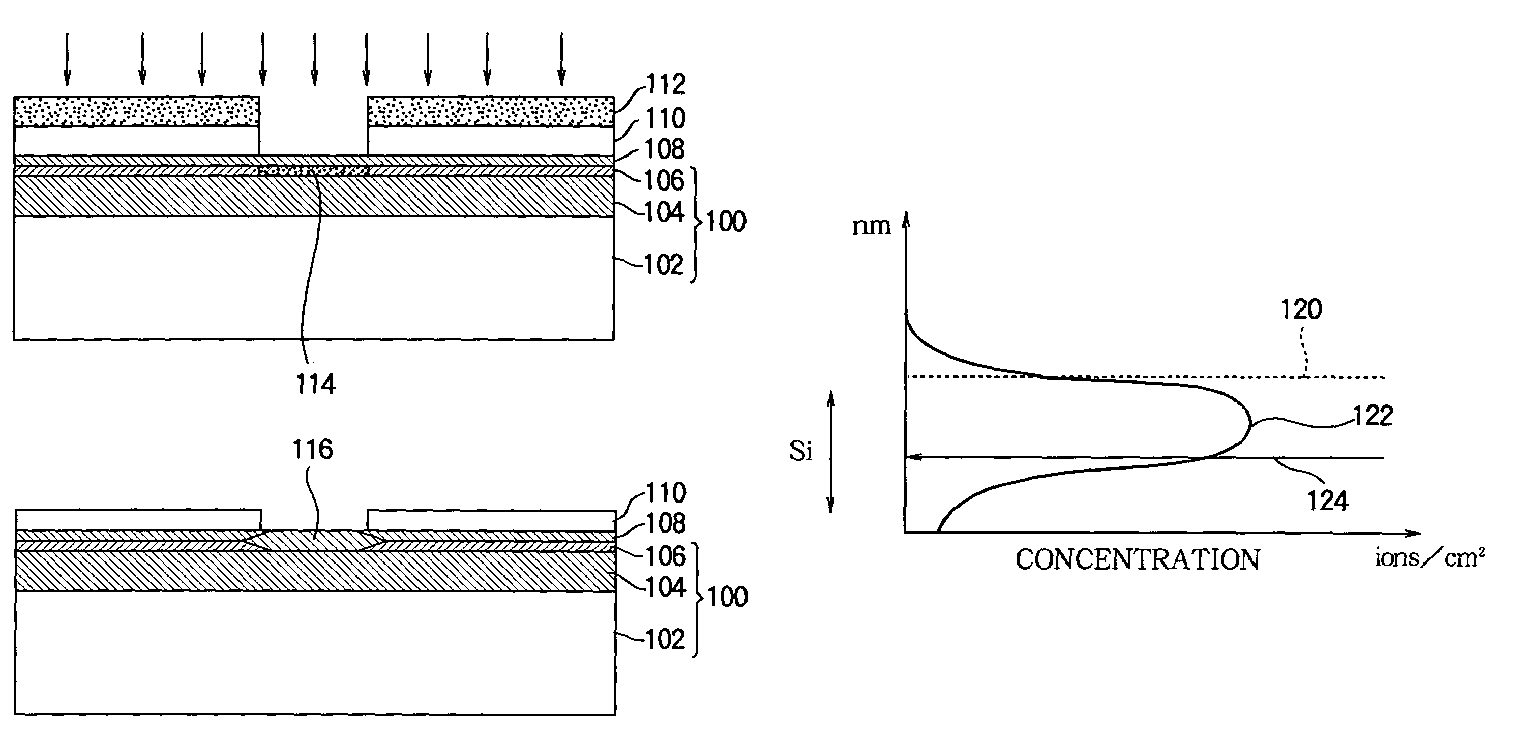
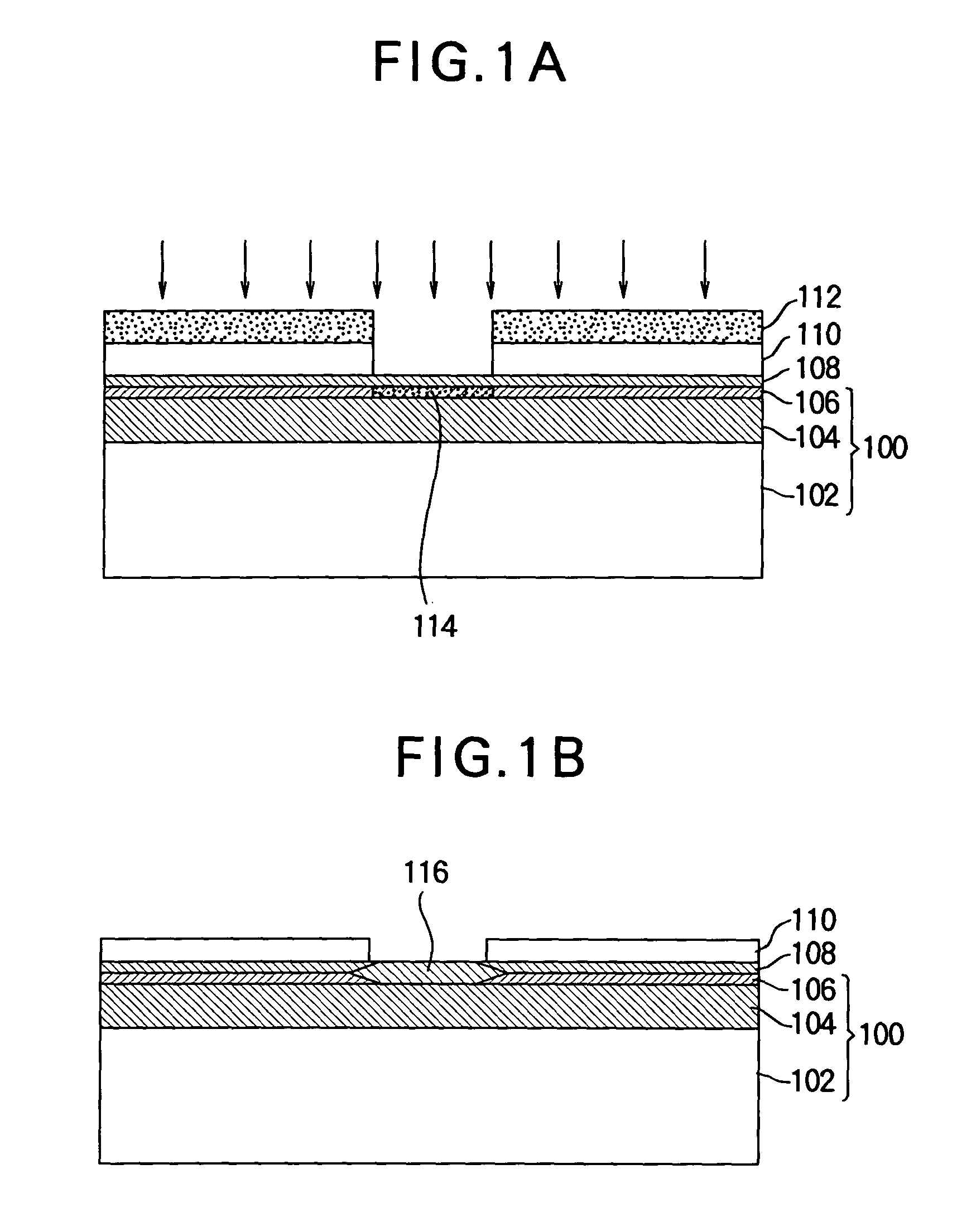
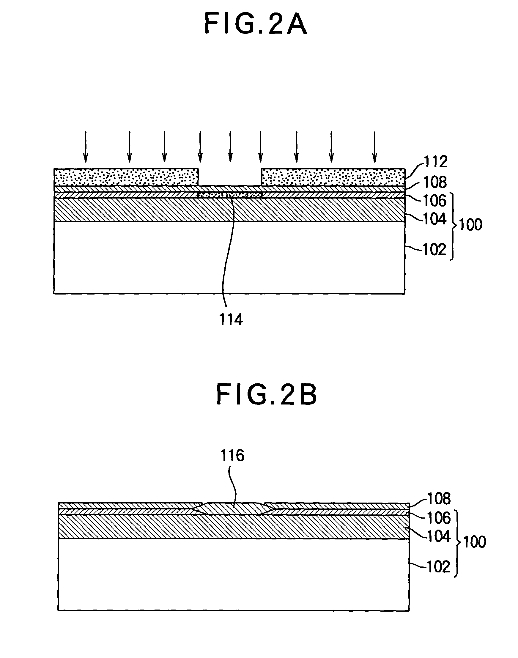
[0022]FIGS. 1A and 1B illustrate the isolation steps in a first embodiment of the invention. An SOI substrate 100 comprising a silicon supporting substrate 102, a buried oxide layer 104, and a silicon layer 106 twenty to seventy nanometers thick is thermally oxidized to form a sacrificial oxide film or pad oxide film 108 five to fifty nanometers thick. This thermal oxidation process reduces the thickness of the silicon layer 106 by an amount that can be precalculated; the thicknesses of the silicon layer 106 and pad oxide film 108 should be selected so that the remaining thickness of the silicon layer 106 and the thickness of the pad oxide film 108 are adequate for later fabrication steps. Next, a nitride film 110 ten to three hundred fifty nanometers thick is formed by chemical vapor deposition (CVD). The purpose of the pad oxide film ...


PUM


Abstract

A method of fabricating a semiconductor device having a silicon layer disposed on an insulating film. Oxygen ions are implanted into selected parts of the silicon layer, which are then oxidized to form isolation regions dividing the silicon layer into a plurality of mutually isolated active regions. As the oxidation process does not create steep vertical discontinuities, fine patterns can be formed easily on the combined surface of the active and isolation regions. The implanted oxygen ions cause oxidation to proceed quickly, finishing before a pronounced bird's beak is formed. The isolation regions themselves can therefore be narrow and finely patterned.

Description

BACKGROUND OF THE INVENTION[0001]1. Field of the Invention[0002]The present invention relates to a semiconductor device fabrication method, and more particularly to the isolation steps in the fabrication method.[0003]2. Description of the Related Art[0004]The most generally used method of isolating circuit elements in a semiconductor device has been local oxidation of silicon (LOCOS) and a variant of this method known as framed local oxidation of silicon (F-LOCOS). In a further variant, proposed in Japanese Unexamined Patent Application Publication No. 7-22504, oxygen ions are implanted into a silicon substrate to form a buried oxide layer (a pad oxide) while maintaining the monocrystalline structure of the silicon above, and this monocrystalline silicon is then selectively oxidized to form a field oxide with smooth transition or ‘bird's-beak’ regions.[0005]Japanese Unexamined Patent Application Publication No. 6-310534 discloses another method in which an impurity of an opposite ty...

Claims


Application Information

Patent Timeline
Patent Type & Authority Patents(United States)
IPC IPC(8): H01L21/76H01L21/316H01L21/762
CPCH01L21/76281H01L21/76264
Inventor KANAMORI, JUN
Owner LAPIS SEMICON CO LTD
Why Eureka
Try Eureka