Flash memory dual in-line memory module management

a memory module and flash memory technology, applied in the field of system and a method managing access to memory, can solve the problems of too slow to be accessed by dimm processors without incurring delays, reads and writes can consume processing cycles and memory bus bandwidth, and achieve the effects of increasing system performance, reducing power consumption, and increasing work capacity

Inactive Publication Date: 2014-04-03
LENOVO ENTERPRISE SOLUTIONS SINGAPORE
View PDF3 Cites 112 Cited by
  • Summary
  • Abstract
  • Description
  • Claims
  • Application Information

AI Technical Summary

Benefits of technology

[0006]An embodiment may avoid expending processor cycles when copying data between the non-coherent flash memory and the coherent DRAM of a DIMM. The processor may thus accomplish other work during the copy operation. The increased work capacity may result in increased system performance. Data transfers may be accomplished without using CPU cycles or initiating traffic on the memory bus to which the DIMM is attached. A system may be able to continue accessing data from the other DIMMs on the memory bus during the copy operation. The data may alternatively remain internal to the DIMM. The internal data transfer may reduce power usage and increase efficiency.
[0007]An embodiment may be compatible with industry standard processors and memory controllers. No logic changes or additional support may be necessary in the processor or memory controller logic. The operating system and / or hypervisor may inhibit or prevent memory accesses to the flash DIMM during the copy procedure to avoid collisions on the use of the DRAM during a copy operation. Accesses to other DIMMs may continue, including DIMMs on the same memory bus as the flash DIMM.

Problems solved by technology

Efforts to incorporate flash memory into dual in-line memory module (DIMM) form factors have been complicated by the underlying NAND technology of flash memory.
NAND memory is not cache coherent and too slow to be accessed by DIMM processors without incurring delays or requiring switching contexts.
Using cache line memory reads and writes can consume processing cycles and memory bus bandwidth.

Method used


Image

  • Flash memory dual in-line memory module management
  • Flash memory dual in-line memory module management
  • Flash memory dual in-line memory module management

Examples


Embodiment Construction

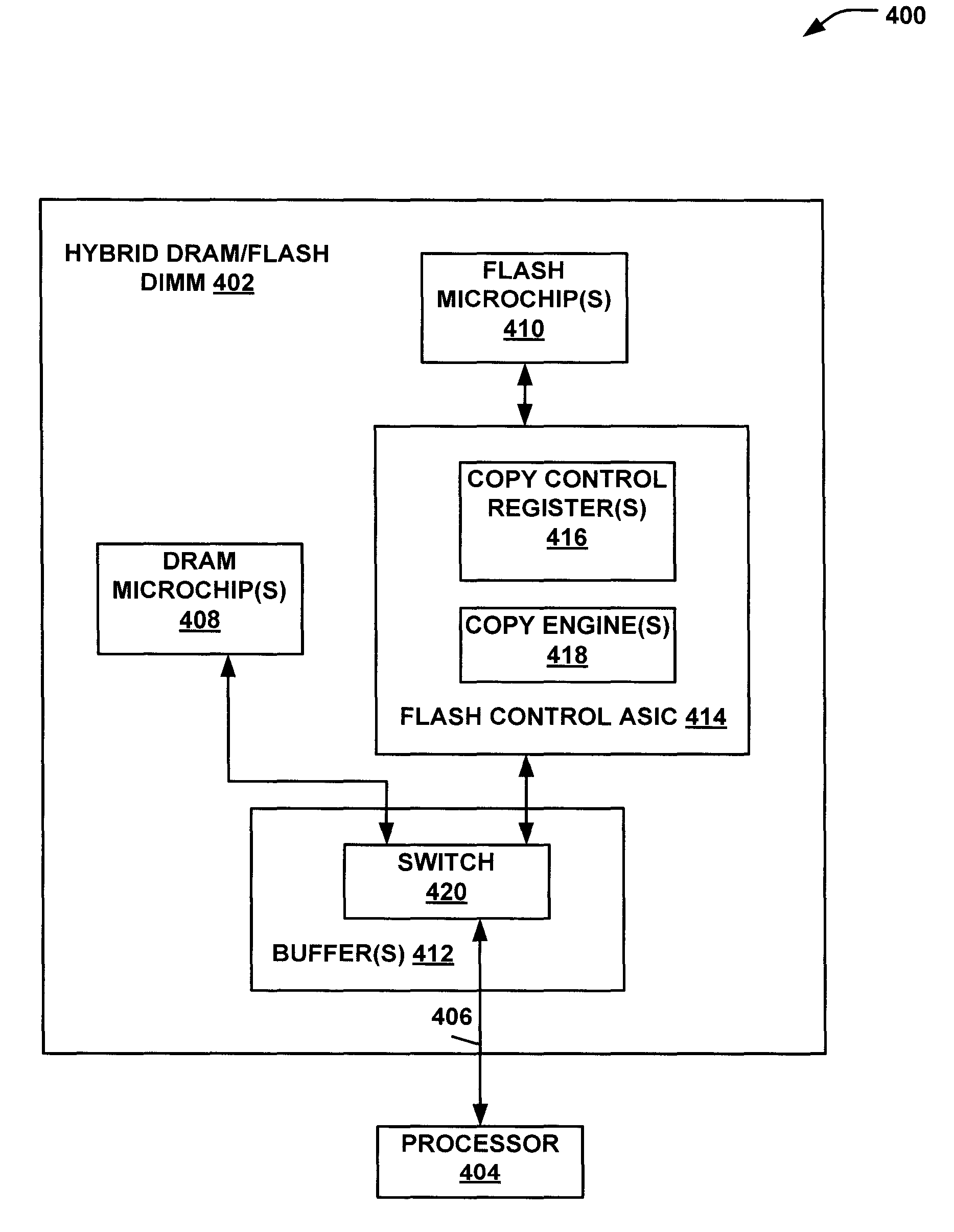
[0014]A dual in-line memory module (DIMM) may be a hybrid of both flash and dynamic random-access memory (DRAM). The DRAM address range may be accessed as standard coherent memory. Flash memory data may be read as non-coherent memory and moved to the DRAM coherent address range to be used as coherent memory by the server. Flash memory DIMM implementations may include buffer chips on the memory bus interface to hide the increased loading of the flash memory. The transfer of data may not use cycles of a central processing unit (CPU) or add traffic to the memory bus to which the DIMM is attached. The cycles of the CPU may thus be available to do work other than copying data. A server or other computing system may be enabled to continue accessing data from the other DIMMs on the memory bus.

[0015]An embodiment may leverage features of a hybrid flash / DRAM DIMM architecture by adding a data path that is internal to the DIMM. For example, an illustrative data path may be added behind the bu...


PUM


Abstract

Systems and methods to manage memory on a dual in-line memory module (DIMM) are provided. A particular method may include receiving at a flash application-specific integrated circuit (ASIC) a request from a processor to access data stored in a flash memory of a DIMM. The data may be transferred from the flash memory to a switch of the DIMM. The data may be routed to a dynamic random-access memory (DRAM) of the DIMM. The data may be stored in the DRAM and may be provided from the DRAM to the processor.

Description

I. FIELD OF THE DISCLOSURE[0001]The present disclosure relates generally to computer memory architectures, and in particular, to a system and a method managing access to memory.II. BACKGROUND[0002]Flash memory is widely used in data centers due for its ability to be electrically erased and reprogrammed. Flash memory is implemented in multiple form factors, such as solid state disk (SSD), as well as on Peripheral Component Interconnect Express (PCIe) flash cards. Efforts to incorporate flash memory into dual in-line memory module (DIMM) form factors have been complicated by the underlying NAND technology of flash memory. NAND memory is not cache coherent and too slow to be accessed by DIMM processors without incurring delays or requiring switching contexts. Using cache line memory reads and writes can consume processing cycles and memory bus bandwidth.III. SUMMARY OF THE DISCLOSURE[0003]In another embodiment, an apparatus may include a flash memory, a dynamic random-access memory (DR...

Claims


Application Information

Patent Timeline
Patent Type & Authority Applications(United States)
IPC IPC(8): G11C16/06G06F12/00
CPCG11C5/04G06F13/1694G06F12/0638Y02D10/00
Inventor BORKENHAGEN, JOHN M.
Owner LENOVO ENTERPRISE SOLUTIONS SINGAPORE
Why Eureka
Try Eureka