Light emission analyzing device

a technology of light emission and analyzing device, which is applied in the direction of instruments, digital computer details, plasma techniques, etc., can solve the problem of difficulty in directly measuring the temperature of the substra

Active Publication Date: 2014-04-17
CREV
View PDF0 Cites 6 Cited by
  • Summary
  • Abstract
  • Description
  • Claims
  • Application Information

AI Technical Summary

Benefits of technology

[0021]The present invention can provide a light emission analyzing device capable of correctly calculating a ratio of light emission intensities between specific two kinds of molecules or atoms.

Problems solved by technology

However, it is difficult to directly measure the substrate temperature.

Method used


Image

  • Light emission analyzing device
  • Light emission analyzing device
  • Light emission analyzing device

Examples


embodiment 1

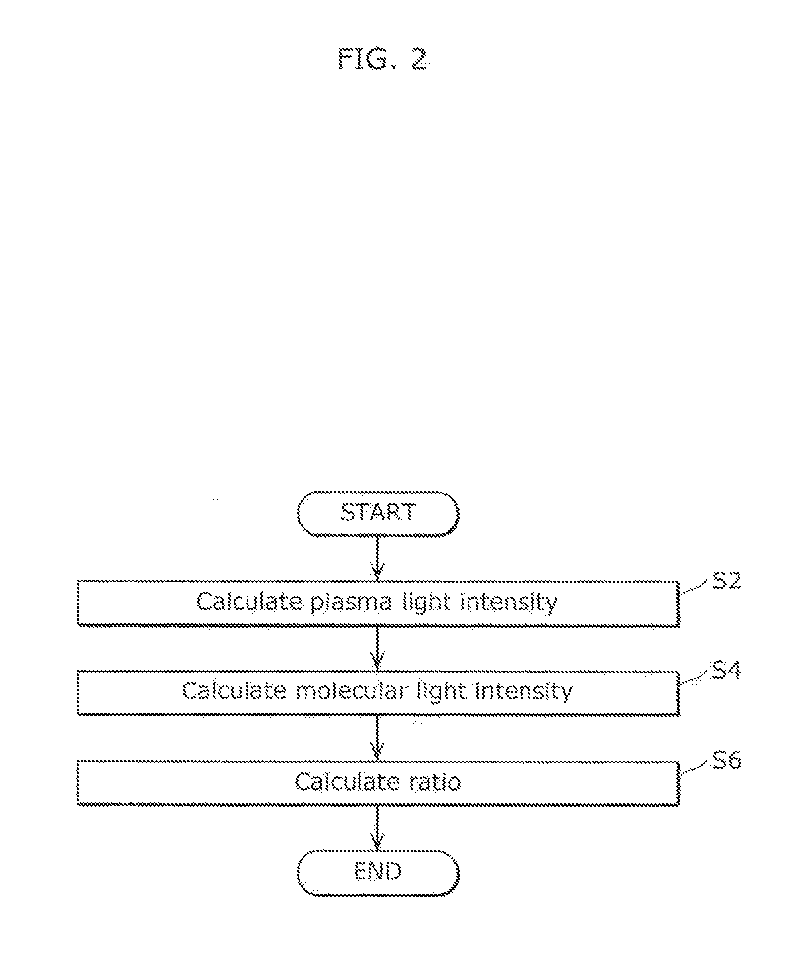
[0035]The following describes a plasma CVD system according to Embodiment 1 of the present invention.

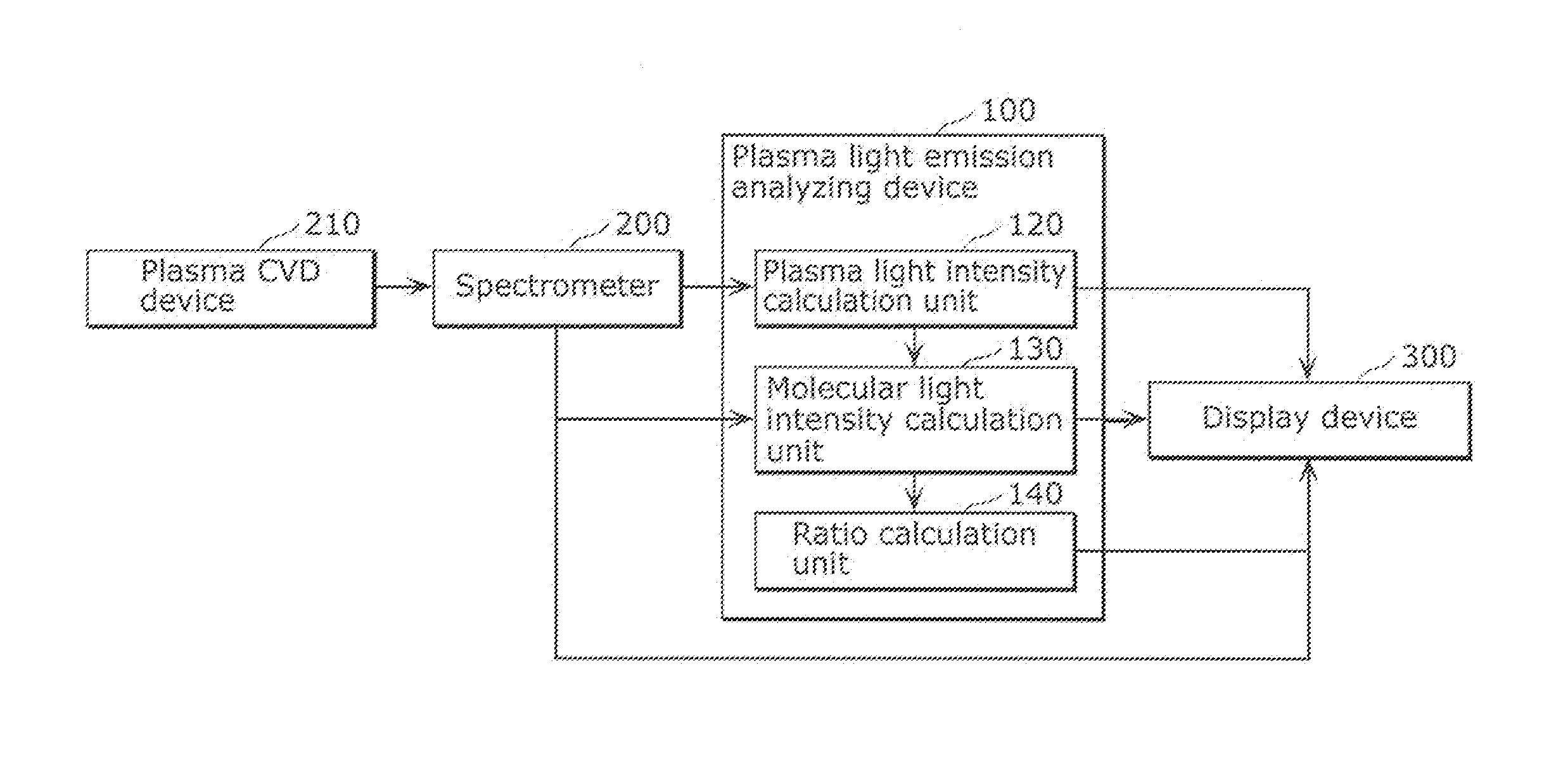
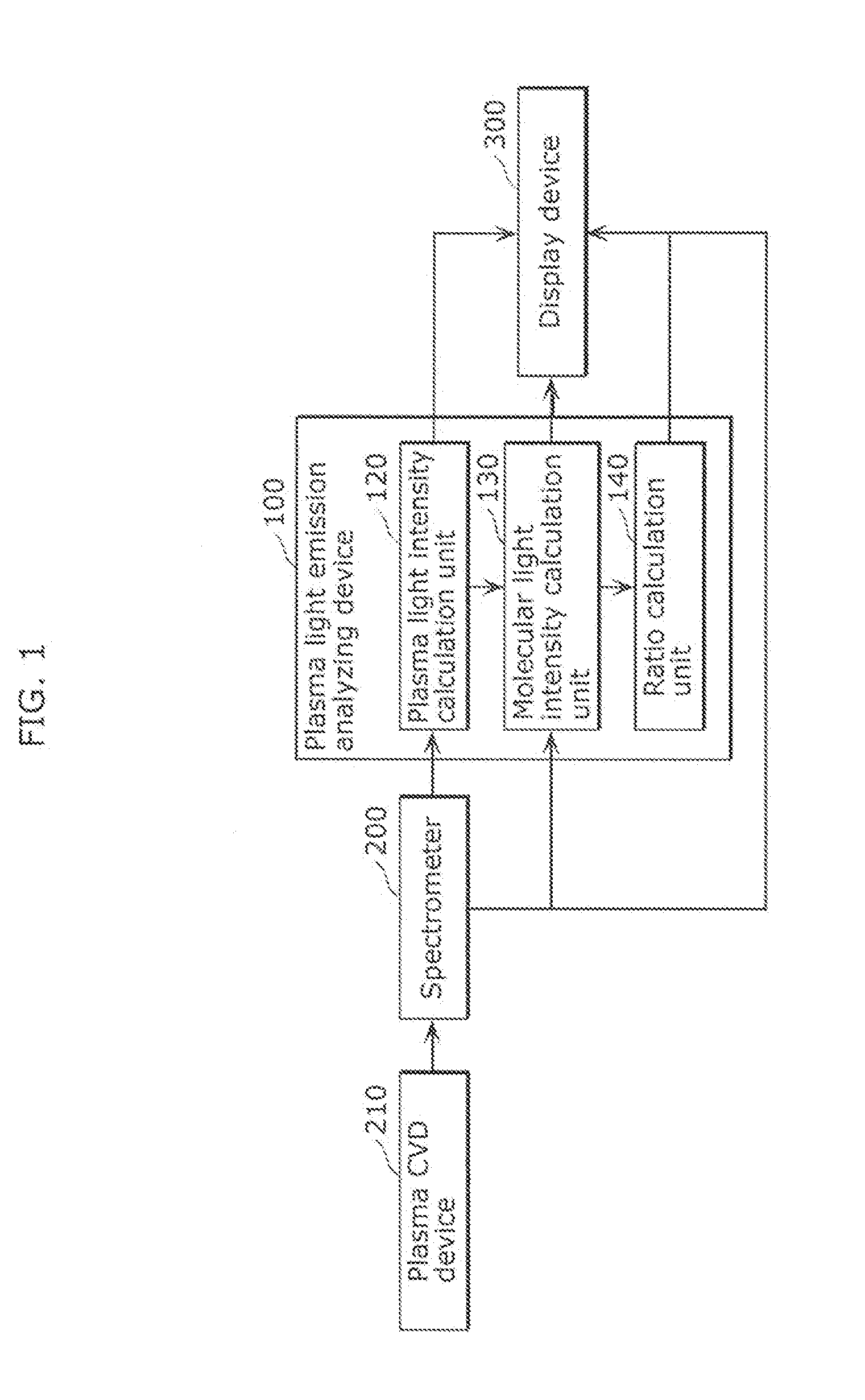
[0036]FIG. 1 is a block diagram showing a functional configuration of the plasma CVD system according to Embodiment 1 of the present invention.

[0037]The plasma CVD system is a system that manufactures thin films on a substrate. The plasma CVD system includes a plasma CVD device 210, a spectrometer 200, a plasma light emission analyzing device 100, a display device 300.

[0038]The plasma CVD device 210 turns a material gas into plasma to form a thin film on / above a substrate. More specifically, the plasma CVD device 210 turns a material gas into plasma in a container to generate active excited molecules, radicals, and ions, thereby facilitating a chemical reaction. As a result, a thin film is formed on / above the substrate.

[0039]The spectrometer 200 measures a spectroscopic spectrum indicating a light intensity for each wavelength in the plasma CVD device 210.

[0040]The plasma light emiss...

embodiment 2

[0056]Next, the description is given for a plasma CVD system according to Embodiment 2 of the present invention.

[0057]The plasma CVD system according to Embodiment 2 differs from the plasma CVD system according to Embodiment 1 in that a light intensity in a predetermined wavelength band is excluded from a spectroscopic spectrum in the plasma CVD device 210 as measured by the spectrometer 200, and polynomial approximation is performed on the spectroscopic spectrum not including the light intensity. The following describes mainly the differences from Embodiment 1.

[0058]FIG. 6 is a block diagram showing a functional configuration of the plasma CVD system according to Embodiment 2 of the present invention. Hereinafter, the same reference numerals in the plasma CVD system according to Embodiment 1 are assigned to identical structural elements in the other figures. The identical structural elements share the same name and the same function, so that their detailed explanations are not repe...


PUM

PropertyMeasurementUnit
wavelengthaaaaaaaaaa
light intensity calculationaaaaaaaaaa

Abstract

The light emission analyzing device includes: a first light intensity calculation unit that performs polynomial approximation on a spectroscopic spectrum indicating a light intensity for each wavelength in a container as measured by a spectrometer so as to calculate the light intensity; a second light intensity calculation unit that subtracts, for each wavelength, the light intensity calculated by the first light intensity calculation unit from the light intensity indicated by the spectroscopic spectrum measured by the spectrometer so as to calculate a light intensity corresponding to a bright-line spectrum of a molecule; and a ratio calculation unit that calculates, by using the light intensity calculated by the second light intensity calculation unit, a ratio between (a) a peak value of a molecular spectrum of a first molecule and (b) a peak value of a molecular spectrum of a second molecule.

Description

TECHNICAL FIELD[0001]The present invention relates to light emission analyzing devices, and more particularly to a light emission analyzing device that analyzes a light emission state in a container measured by a spectrometer.BACKGROUND ART[0002]In forming films by using plasma Chemical Vapor Deposition (CVD) devices, it is important to suppress generation of fine particles called powder (for example, see Patent Literature (PTL) 1: Japanese Unexamined Patent Application Publication No. 2004-296526). The suppression of power generation requires measurement of a substrate temperature. However, it is difficult to directly measure the substrate temperature. In order to address this, a ratio of light emission intensities between a silicon* (Si*) film and a silan* (SiH*) film (where “*” represents an atomic valence) which are formed above the substrate is calculated as a value related to the substrate temperature. Such a conventional plasma CVD device controls a gas flow rate in the plasm...

Claims


Application Information

Patent Timeline
Patent Type & Authority Applications(United States)
IPC IPC(8): G01N21/25
CPCG01N21/255G01J3/443H05H1/0037G01J2003/4435G01N21/274G01N21/66G01N2201/127
Inventor YAMASHITA, MASAKIMIZUKAWA, HIROMI
Owner CREV
Why Eureka
Try Eureka