Error correction code circuit and memory device including the same

a code circuit and error correction technology, applied in the field of error correction code circuit and memory device, can solve the problems of increasing error rate and increasing error bit generation ra

Active Publication Date: 2014-04-17
SAMSUNG ELECTRONICS CO LTD
View PDF18 Cites 11 Cited by
  • Summary
  • Abstract
  • Description
  • Claims
  • Application Information

AI Technical Summary

Benefits of technology

[0013]Embodiments may provide an error correction code (ECC) circuit including a search unit configured to determine whether there is an error in each bit of a data sequence by using an arbitrary element on a Galois Field GF(2m), where m is an integer, as a substitution value, wherein the search unit includes a basis calculating unit that generates basis vectors from elements that are linearly independent on the Galois Field GF(2m) based on an error locator polynomial that is a linear function using the substitution value; and a linear expansion unit that calculates remaining elements that are not linearly independent on the Galois Field by performing XOR operations on results output from the basis calculating unit using the substitution value, wherein a number of XOR elements in the linear expansion unit for performing the XOR operations is less than (n+1)×(2m−1)×m(m−1) / 2+n×(2m−1)×m, where n is an order of the error locator polynomial.

Problems solved by technology

For example, due to degradation of a tunnel oxide layer according to several times of a rewrite operation, a memory cell loses data retaining characteristics while retaining data, and an error bit generation rate (error rate) tends to increase.
In particular, in relation to the NAND flash memory, as a large capacity memory and a micronized manufacturing process are developed, the error rate tends to increase.

Method used


Image

  • Error correction code circuit and memory device including the same
  • Error correction code circuit and memory device including the same
  • Error correction code circuit and memory device including the same

Examples


Embodiment Construction

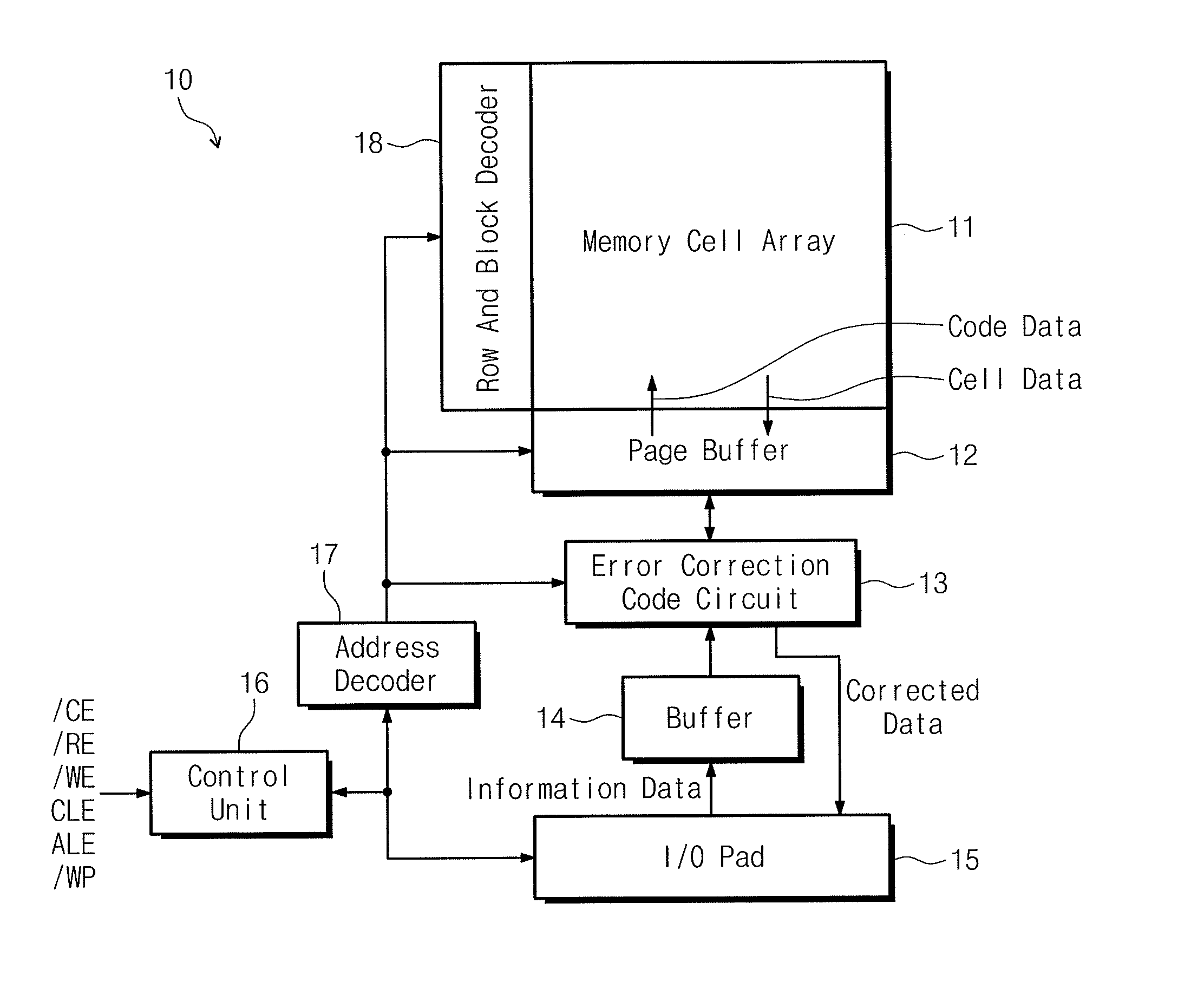
[0030]Example embodiments will now be described more fully hereinafter with reference to the accompanying drawings; however, they may be embodied in different forms and should not be construed as limited to the embodiments set forth herein. Rather, these embodiments are provided so that this disclosure will be thorough and complete, and will fully convey exemplary implementations to those skilled in the art.

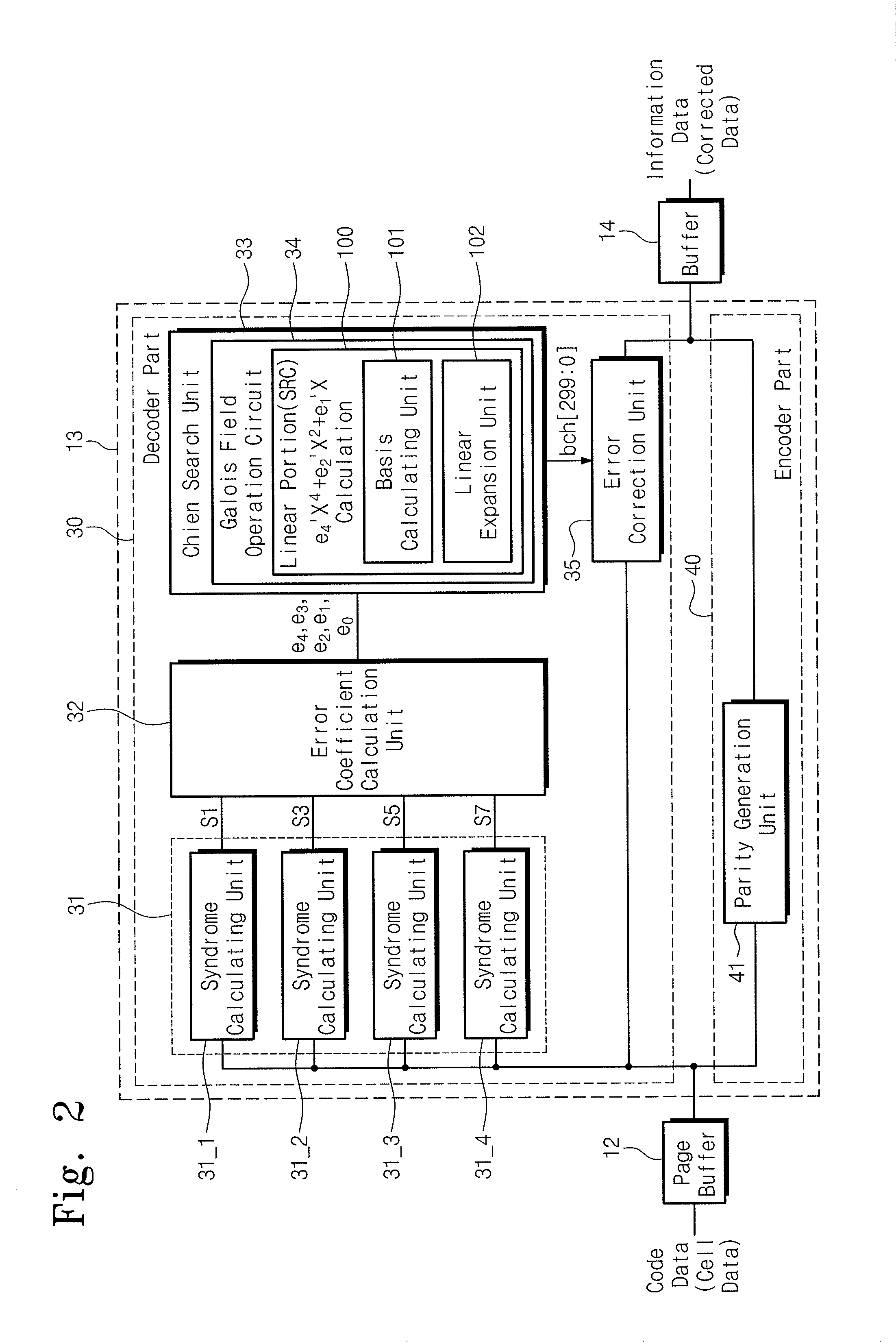
[0031]In a typical Galois Field operation circuit, for example, in a circuit (a circuit for 4th order polynomial) shown in FIG. 12, after coefficients (e0, e1, e2, e3, e4) of an error locator polynomial P(X), roots of P(X) are obtained by sequentially inputting 1(=α0), α(=α1), α2, α3, . . . , as a Galois field element X. In detail, in a Galois Field operation circuit 34B for obtaining roots of a typical Galois Field polynomial, firstly, coefficients e1(i=0, 1, 2, 3, 4) are calculated; secondly, a term e1Xi is calculated; and, thirdly, each term corresponding to 1=0, 1, 2, 3, 4 is...


PUM


Abstract

The ECC circuit includes a Chien search unit configured to determine whether there is an error in each bit of a data sequence. The Chien search unit selects a coefficient of a nonlinear term from among terms of an error locator polynomial as a nonlinear coefficient, separates the error locator polynomial into a first location equation including only linear terms and a second location equation including only nonlinear terms, determines a third location equation by dividing the first location equation by the nonlinear coefficient, determines a fourth location equation by dividing the second location equation by the nonlinear coefficient, and determines whether there is an error for each of the bits by performing an XOR operation on a result of the third location equation using the substitution value and a result of the fourth location equation using an arbitrary element of the error locator polynomial as a substitution value.

Description

CROSS-REFERENCE TO RELATED APPLICATION[0001]Japanese Patent Application No. 2012-227834, filed on Oct. 15, 2012, in the Japanese Intellectual Property Office, and entitled: “Error Correction Code Circuit and Memory Device Including the Same,” is incorporated by reference herein in its entirety.BACKGROUND[0002]1. Field[0003]Embodiments relate to an error correction code circuit and a memory device including the same.[0004]2. Description of the Related Art[0005]A NAND flash memory is one of electrically erasable and programmable read only memories (EEPROMs). The NAND flash memory enables large amounts of data to be stored in a small chip area by using NAND cell units (NAND strings) in which a plurality of memory cells are serially connected.[0006]In relation to a large capacity memory device such as the NAND flash memory, retained data disappear sometimes due to various causes. For example, due to degradation of a tunnel oxide layer according to several times of a rewrite operation, a...

Claims


Application Information

Patent Timeline
Patent Type & Authority Applications(United States)
IPC IPC(8): H03M13/07
CPCH03M13/07H03M13/1515H03M13/152H03M13/1545H03M13/158H03M13/19G06F11/10G06F12/00G06F11/08G06F11/1008G06F11/1048G06F11/1068G11C29/04H03M13/1148H03M13/151H03M13/153H03M13/154H03M13/1575H03M13/3707H03M13/6566
Inventor FUJIWARA, DAISUKE
Owner SAMSUNG ELECTRONICS CO LTD
Why Eureka
Try Eureka