Substrate and Method for Cutting the Substrate

a substrate and substrate technology, applied in the direction of electrical equipment, semiconductor devices, semiconductor/solid-state device details, etc., can solve the problems of increasing the workload of personnel, achieve the effect of reducing the errors of inspection equipment, accelerating the cutting speed of substrate, and reducing the gradient and taper on the cutting edg

Inactive Publication Date: 2014-04-24
SHENZHEN CHINA STAR OPTOELECTRONICS TECH CO LTD
View PDF0 Cites 1 Cited by
  • Summary
  • Abstract
  • Description
  • Claims
  • Application Information

AI Technical Summary

Benefits of technology

[0023]By creating an etching groove on the first surface of the first sheet and a third surface of the second sheet, the cutting depth of the substrate is properly and vertically reduced. As a result, the cutting speed of the substrate can be accelerated. The gradient and taper on the cutting edge are also reduced so as to reduce the errors of the inspecting equipments. In addition, the workload of the personnel can also be lowered.

Problems solved by technology

1. When the pressure is applied on the opposite surface of the substrate 200, extension of the scored groove could be tilted or offset from its original direction.
2. The substrate 200 is configured with a thin-film transistor liquid crystal panel and a color filter substrate, once the taper of the thin-film transistor liquid crystal panel and the color filter substrate are different, a gradient could be formed therebetween.
3. The taper or gradient could fall within the specification, however, during the field inspection, the equipment could make an error in view of that. Accordingly, this will inevitably increase the workload of the personnel.

Method used


Image

  • Substrate and Method for Cutting the Substrate
  • Substrate and Method for Cutting the Substrate
  • Substrate and Method for Cutting the Substrate

Examples


Embodiment Construction

[0028]Detailed description will he given to the embodiments along with the accompanied drawings.

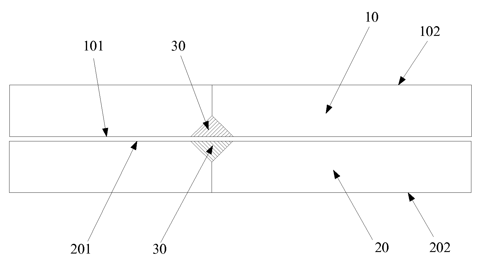
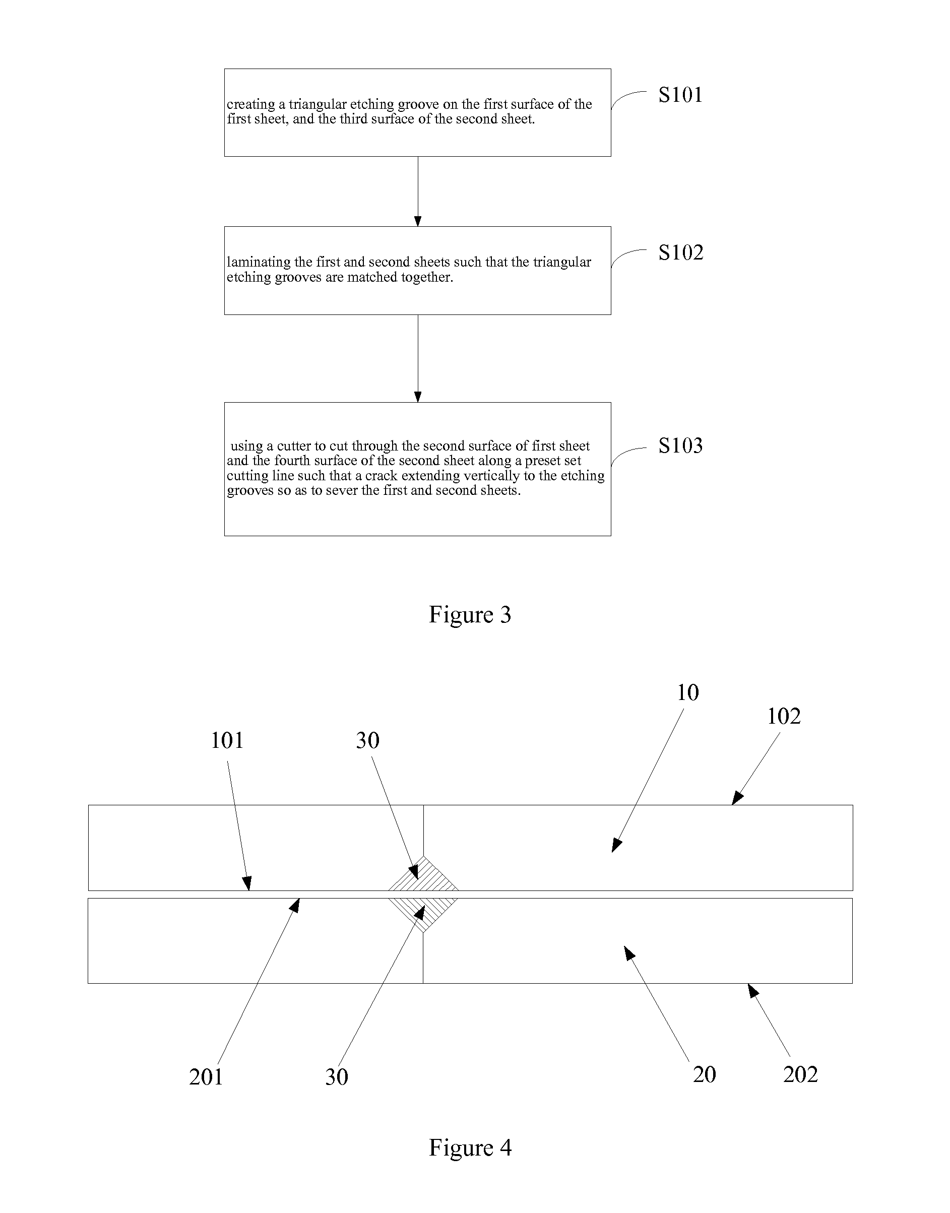
[0029]Referring to FIG. 3, which is a flow diagram of a method for cutting substrate made in accordance with the present invention. The substrate is configured with a first sheet having a first surface and a second surface opposite to the first surface, and a second sheet having a third surface and a fourth surface opposite to the third surface. The first sheet is a thin-film transistor liquid crystal display, and the second sheet is a color filter substrate. Of course, the first sheet can he a color filter sheet, and the second sheet can he the thin-film transistor liquid crystal display. No limitation should be imposed thereon. The method of cutting the substrate includes the steps of following.

[0030]Step S101: creating a triangular etching groove on the first surface of the first sheet, and the third surface of the second sheet.

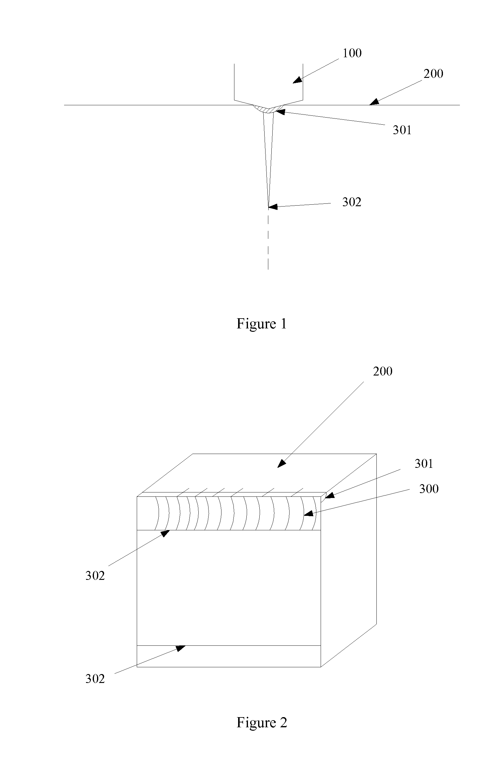
[0031]In the current embodiment, it is preferable to have ...


PUM


Abstract

The present invention discloses a method for cutting a substrate. The method includes the steps of 1) creating a etching groove in the first surface of the first sheet and the third surface of the second sheet; 2) laminating the first and second sheets with the etching grooves aligned with each other; and 3) using a cutter to cut through the second surface of first sheet and the fourth surface of the second sheet along a preset set cutting line such that a crack extending vertically to the etching grooves so as to sever the first and second sheets. The present invention further discloses a substrate. By way of the foregoing, the taper and gradient along the cutting edge can be reduced.

Description

[0001]The present invention relates to a technical field of liquid crystal display device, and more particularly w a substrate and at method for cutting the substrate.BACKGROUND OF THE INVENTION[0002]Currently, the severance of the liquid substrate is made by cutting wheel. As shown in FIGS. 1 and 2, in which FIG. 1 is a working principle of a method for cutting a substrate; and FIG. 2 is a cross sectional view shown the substrate after severance. The substantial cutting procedures is 1) applying the cutting, wheel 100 toward a surface of the substrate 200 such that the surface is scored with a groove 300 which divides into a horizontal groove 300 and vertical groove 302. Then, pressure is applied on the opposite surface so as to extend the vertical groove 320 (dotted line in FIG. 1). Then the substrate is severed.[0003]However, the existing cutting method inherits the potential problems.[0004]1. When the pressure is applied on the opposite surface of the substrate 200, extension of...

Claims


Application Information

Patent Timeline
Patent Type & Authority Applications(United States)
IPC IPC(8): H01L21/78H01L23/544
CPCH01L23/544H01L21/78H01L2223/54426H01L2223/5446H01L2924/0002H01L2924/00
Inventor CHEN, HSIN-HUA
Owner SHENZHEN CHINA STAR OPTOELECTRONICS TECH CO LTD
Why Eureka
Try Eureka