Light-Emitting Panel, Display Device, and Method for Manufacturing Light-Emitting Panel
- Summary
- Abstract
- Description
- Claims
- Application Information
AI Technical Summary
Benefits of technology
Problems solved by technology
Method used
Image

Examples
embodiment 1
[0045]An object of one embodiment of the present invention is to provide a novel light-emitting panel in which a decrease in aperture ratio accompanied by fabrication of a high-definition panel is prevented.
[0046]In a manufacturing process of a light-emitting panel, there is a possibility that misalignment may occur. In the case of providing a space in a light-emitting panel allowing for the misalignment, the following points should be noted.
[0047]First, a large space is necessary to allow for misalignment as compared to the other technology for selectively forming thin films (e.g., photolithography, nanoimprint lithography), in a step of selectively forming layers containing light-emitting organic compounds.
[0048]Second, as the number of layers containing light-emitting organic compounds, which are formed selectively, increases, the space for allowing misalignment needs to be larger.
[0049]Third, a step that may cause damage to the layers containing light-emitting organic compounds ...
embodiment 2
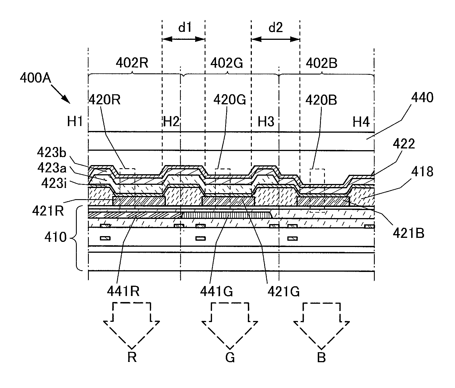
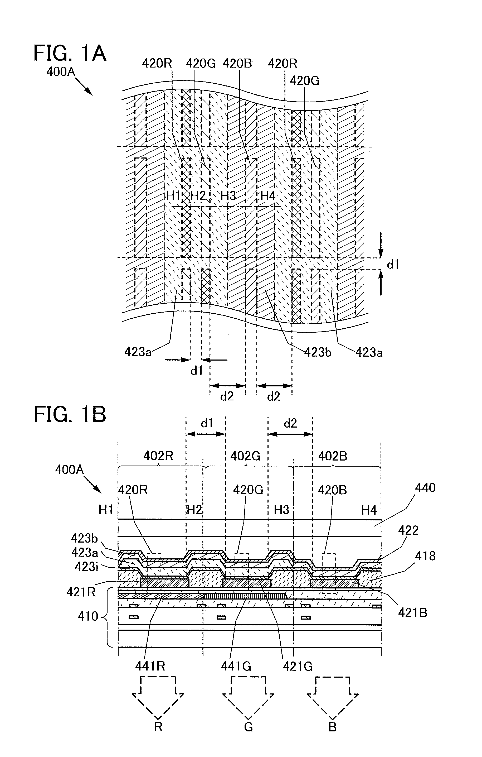
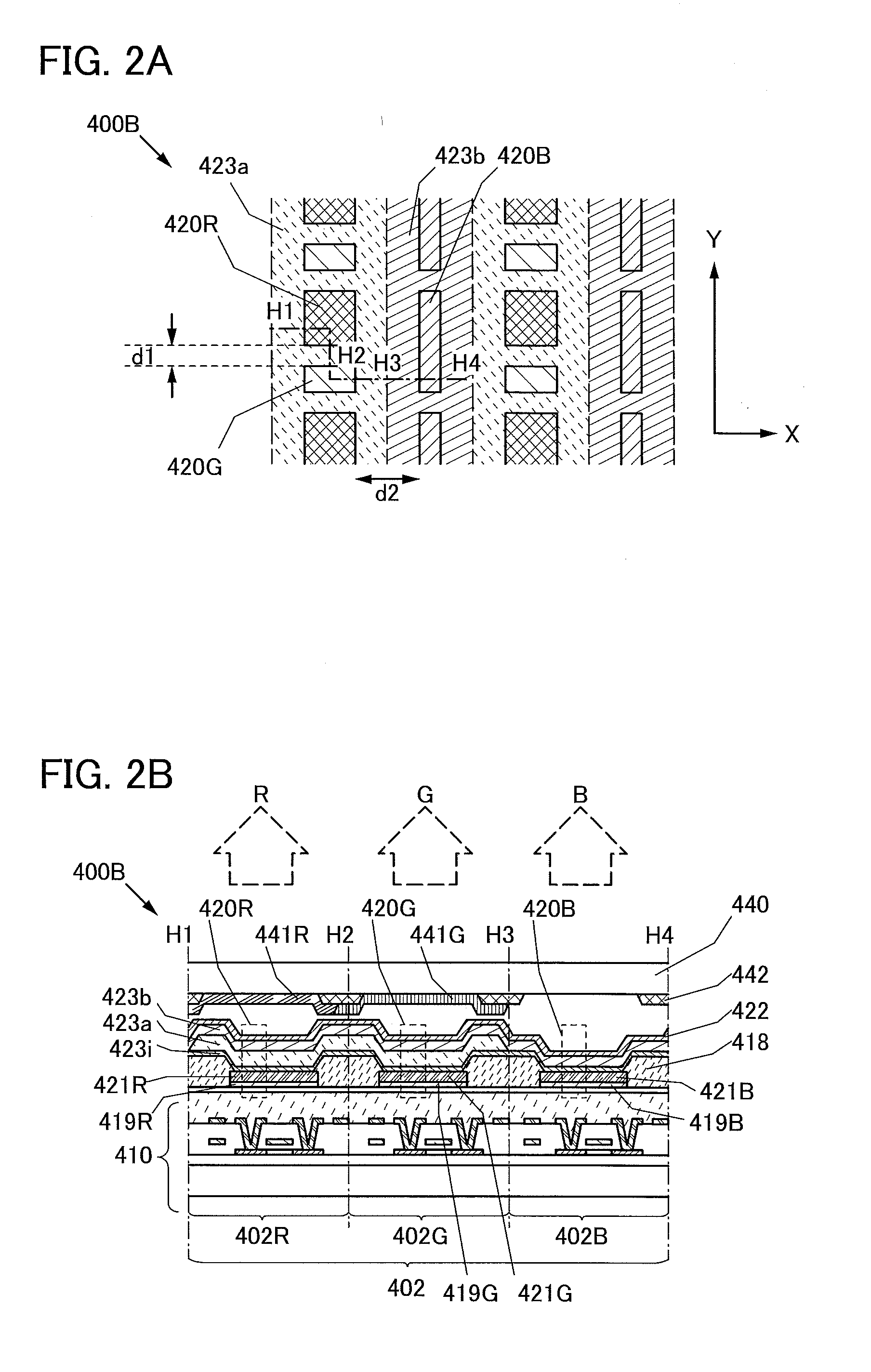
[0107]In this embodiment, structures of a light-emitting panel of one embodiment of the present invention will be described with reference to FIGS. 2A and 2B, FIG. 3, and FIGS. 8A1, 8A2, 8B1, and 8B2.
[0108]FIG. 2A is a top view of a structure of the light-emitting panel of one embodiment of the present invention, and FIG. 2B is a side view of the structure of the light-emitting panel along line H1-H2-H3-H4 in FIG. 2A.
[0109]FIG. 3 is a top view of a structure of the light-emitting panel of one embodiment of the present invention.
[0110]FIGS. 8A1, 8A2, 8B 1, and 8B2 are top views for describing the relationship between misalignment and the layout of light-emitting elements in sub-pixels and a space between the light-emitting elements in a light-emitting panel.
[0111]In a light-emitting panel 400B described in this embodiment as an example, a first sub-pixel 402R, a second sub-pixel 402G and a third sub-pixel 402B are included over a substrate 410.
[0112]The first sub-pixel 402R includes ...
embodiment 3
[0179]In this embodiment, a structure of a light-emitting panel of one embodiment of the present invention will be described with reference to FIGS. 4A and 4B.
[0180]FIG. 4A is a top view of the structure of the light-emitting panel of one embodiment of the present invention, and FIG. 4B is a side view of the structure of the light-emitting panel along line H1-H2-H3-H4 in FIG. 4A.
[0181]A light-emitting panel 400D described in this embodiment as an example has the structure described below in addition to the structure of the light-emitting panel 400C described in Embodiment 2 (see FIG. 4B).
[0182]The light-emitting elements (the first light-emitting element 420R, the second light-emitting element 420G, and the third light-emitting element 420B) include the second layer 423b containing the light-emitting organic compound between their respective pairs of electrodes (specifically, between the first lower electrode 421R and the upper electrode 422, between the second lower electrode 421G ...
PUM
 Abstract
Description
Claims
Application Information
 - Generate Ideas
- Intellectual Property
- Life Sciences
- Materials
- Tech Scout
- Unparalleled Data Quality
- Higher Quality Content
- 60% Fewer Hallucinations
Browse by: Latest US Patents, China's latest patents, Technical Efficacy Thesaurus, Application Domain, Technology Topic, Popular Technical Reports.
© 2025 PatSnap. All rights reserved.Legal|Privacy policy|Modern Slavery Act Transparency Statement|Sitemap|About US| Contact US: help@patsnap.com