Method of detecting the circular uniformity of the semiconductor circular contact holes

Active Publication Date: 2014-05-08
SHANGHAI HUALI MICROELECTRONICS CORP
View PDF6 Cites 7 Cited by
  • Summary
  • Abstract
  • Description
  • Claims
  • Application Information

AI Technical Summary

Benefits of technology

[0021]The advantages of the present invention are: the circular uniformity of the contact holes are reflected effectively and comprehensively, the

Problems solved by technology

With the development of semiconductor technology and the miniaturization in the feature size of device, the requirements on accuracy and stability during the production process are increasingly strict, even a deviation of a few nanometers can cause the yield loss.
During the process whose feature size is 45 nanometers and below, the accuracy problem of the feature size may indirectly cause that the semiconductor device performance deviates from the normal values, for example it might cause an electric leakage, etc.
In some more serious situation, it can even result to the device failure, for example, short-circuit will be caused by the too small distance between contact holes.
The measure m

Method used


Image

  • Method of detecting the circular uniformity of the semiconductor circular contact holes
  • Method of detecting the circular uniformity of the semiconductor circular contact holes
  • Method of detecting the circular uniformity of the semiconductor circular contact holes

Examples


Example

[0025]The present invention will be further illustrated as follows in combination with the figures and the embodiments, but these contents should not be deemed as the limitation of this invention.

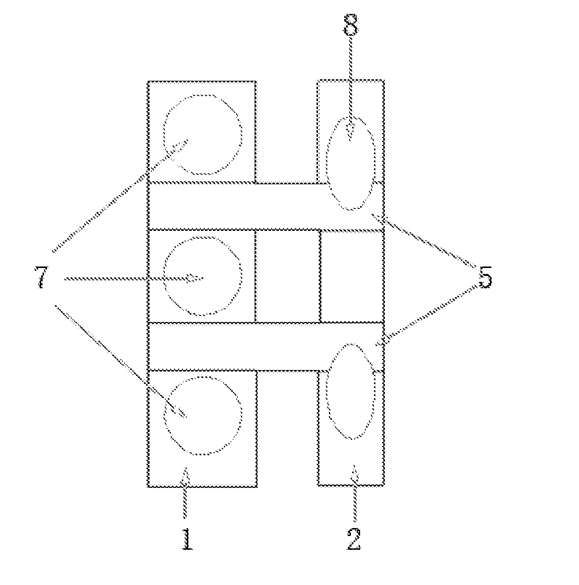
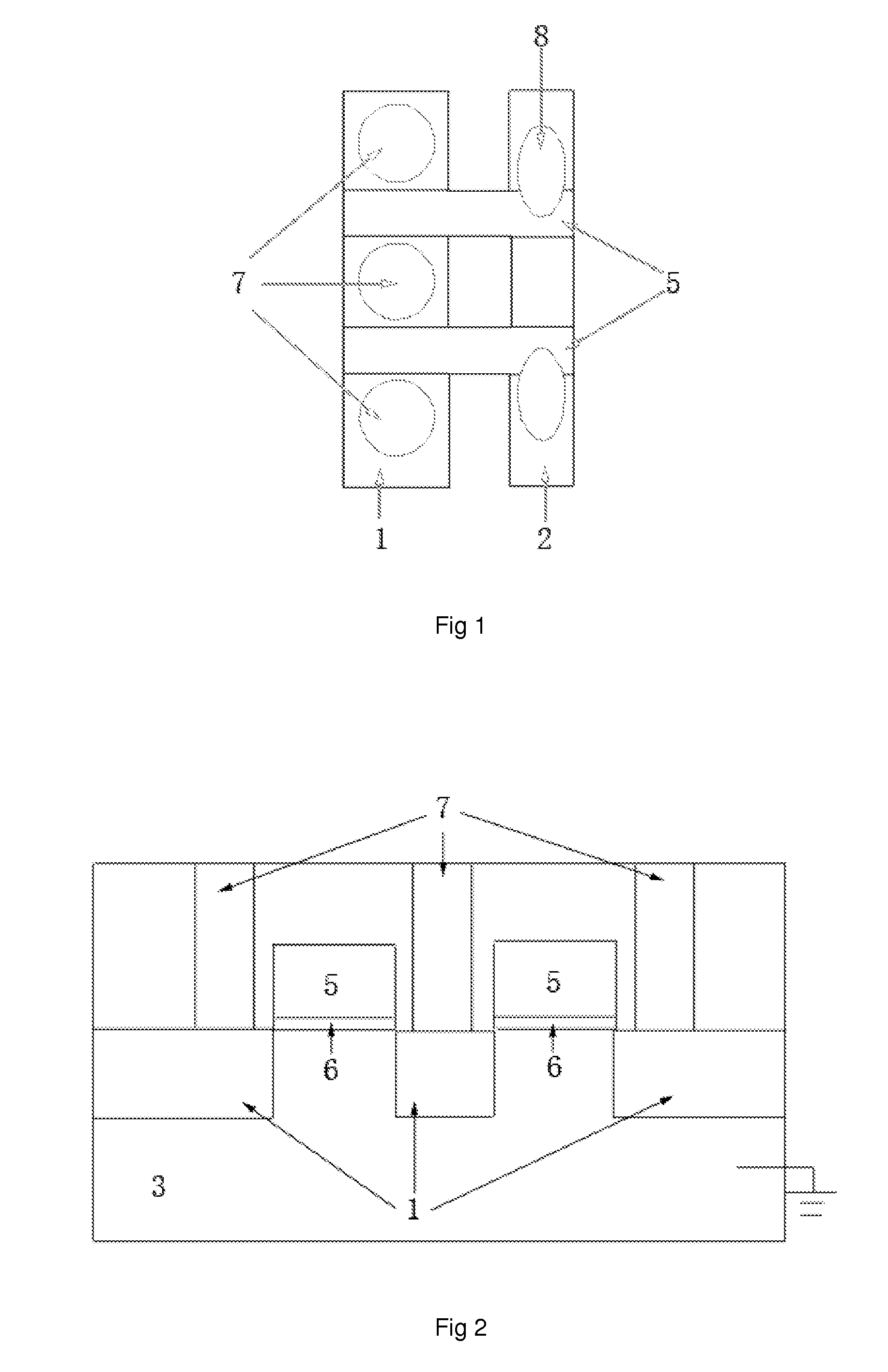
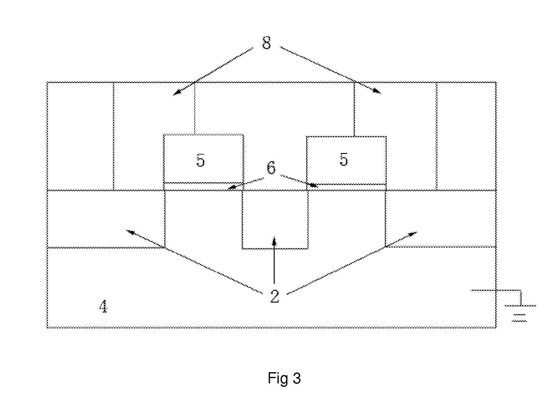
[0026]As shown in FIG. 1, it is a detection circuit structure which is applied in detecting and checking the circular uniformity of the semiconductor circular contact holes in the embodiment of the present invention. The detection circuit structure includes an N-type active region 1 and a P-type active region 2 which are separated by a silicon dioxide layer, wherein the N-type active region 1 is in a P well 3 (as shown in FIG. 2) and the P-type active region 2 is in an N well 4 (as shown in FIG. 3). A polysilicon gate 5 bridges the N-type active region and the P-type active region, gate oxide layers are disposed between the P-type active regions and the N-type active regions to insulate the P-type regions and the N-type regions from the polysilicon gates (as shown in FIGS. 2 and 3) so that ...


PUM


Abstract

A method of detecting the circular uniformity of semiconductor circular contact holes. Several detection circuit structures are disposed on the semiconductor wafer: N-type active regions and P-type active regions; silicon dioxide layers separate the N-type active regions from the P-type active regions; the N-type active regions are formed in the P well and the P-type active regions are formed in the N well; polysilicon gates bridge the N-type active regions and the P-type active regions; gate oxide layers insulate the P-type regions and the N-type regions from the polysilicon gates, so that the P-type regions and the N-type regions are independent; the N-type active regions connect with circular contact holes while the P-type active regions and the polysilicon gates connect with oval contact holes; a electron beam scanner detects the circular uniformity of the contact holes. This invention advantageously reflects effectively and comprehensively the circular uniformity of the contact holes.

Description

CROSS-REFERENCE TO RELATED APPLICATIONS[0001]The present application claims priority under 35 U.S.C. §119 and the Paris Convention to Chinese application number CN 201210432250.3, filed on Nov. 2, 2012, the disclosure of which is herewith incorporated by reference in its entirety.FIELD OF THE INVENTION[0002]The present invention relates to the field of semiconductor fabrication, in particular it relates to a method of detecting the circular uniformity of semiconductor circular contact holes.BACKGROUND OF THE INVENTION[0003]With the development of semiconductor technology and the miniaturization in the feature size of device, the requirements on accuracy and stability during the production process are increasingly strict, even a deviation of a few nanometers can cause the yield loss. Especially, the feature sizes of polysilicon gates and circular contact holes are more sensitive. Circular uniformity is one of the technical parameters of the circular contact holes in the technical sta...

Claims


Application Information

Patent Timeline
IPC IPC(8): H01L21/66
CPCH01L22/12H01L2924/0002Y10S257/911Y10S257/912H01L2924/00
Inventor WANG, KAICHEN, HUNGLINLONG, YINNI, QILIANGKUO, MINGSHEN
Owner SHANGHAI HUALI MICROELECTRONICS CORP
Why Eureka
Try Eureka