Interconnection matrix using semiconductor non-volatile memory

a non-volatile memory and interconnection matrix technology, applied in the field of interconnection matrixes, can solve the problems of prolonging the development time, and reducing the quality of interconnection matrix using sglnvm

Active Publication Date: 2014-05-22
FLASHSILICON
View PDF5 Cites 7 Cited by
  • Summary
  • Abstract
  • Description
  • Claims
  • Application Information

AI Technical Summary

Benefits of technology

[0013]FIG. 2 shows the drain current versus control gate voltage characteristic curves for programmed and erased cells for N-type Scalable Gate Logic Non-Volatile Memory (SGLNVM) devices according to one embodiment of the invention. FIG. 3 shows the Ron (transistor “on” resistance) versus sunk current characteristic curves at 1.2 V voltage bias with various applied control gate voltages Vcg for an erased N-type SGLNVM device according to one embodiment of the invention. The Ron is in the range of tens kΩ in comparison with those of ˜MΩ for oxide-breaking anti-fuses (for instance see U. S. Pat. No. 7,825,479 B2). Thus, in term of propagating delay speeds, the quality of interconnection matrix using SGLNVM is better than those using oxide-breaking anti-fuse.

Problems solved by technology

Once the final hard wiring process is completed the circuitry is not able to change without re-masking and re-processing on the new silicon.
Lack of flexibility of changing the wiring configuration after fabrication the hard wiring methodology usually results in the development cost increase for mask revision and silicon re-fabrication, and further prolongs the development time.
On the other hand, OTP types of fuses (anti-fuses) are not able to provide viable solutions for the applications requiring large configurable wiring capacity such as Field Programmable Array (FPA) and multiple configurable I / Os (input / output pads).
Using large amounts of OTP fuses (anti-fuses) for the multiple times configurable wiring capacity in IC chips become unrealistic costly.
Furthermore, the low core operational voltages of the modern IC chips are coincident with the required low voltages for applying to the drain electrodes of non-volatile memory devices without disturbing the devices' threshold voltages from the drain hot carrier injection, a phenomenon known as the read disturbance from applying high drain voltages.

Method used


Image

  • Interconnection matrix using semiconductor non-volatile memory
  • Interconnection matrix using semiconductor non-volatile memory
  • Interconnection matrix using semiconductor non-volatile memory

Examples


Embodiment Construction

[0021]The following detailed description is meant to be illustrative only and not limiting. It is to be understood that other embodiment may be utilized and element changes may be made without departing from the scope of the present invention. Also, it is to be understood that the phraseology and terminology used herein are for the purpose of description and should not be regarded as limiting. Those of ordinary skill in the art will immediately realize that the embodiments of the present invention described herein in the context of methods and schematics are illustrative only and are not intended to be in any way limiting. Other embodiments of the present invention will readily suggest themselves to such skilled persons having the benefits of this disclosure.

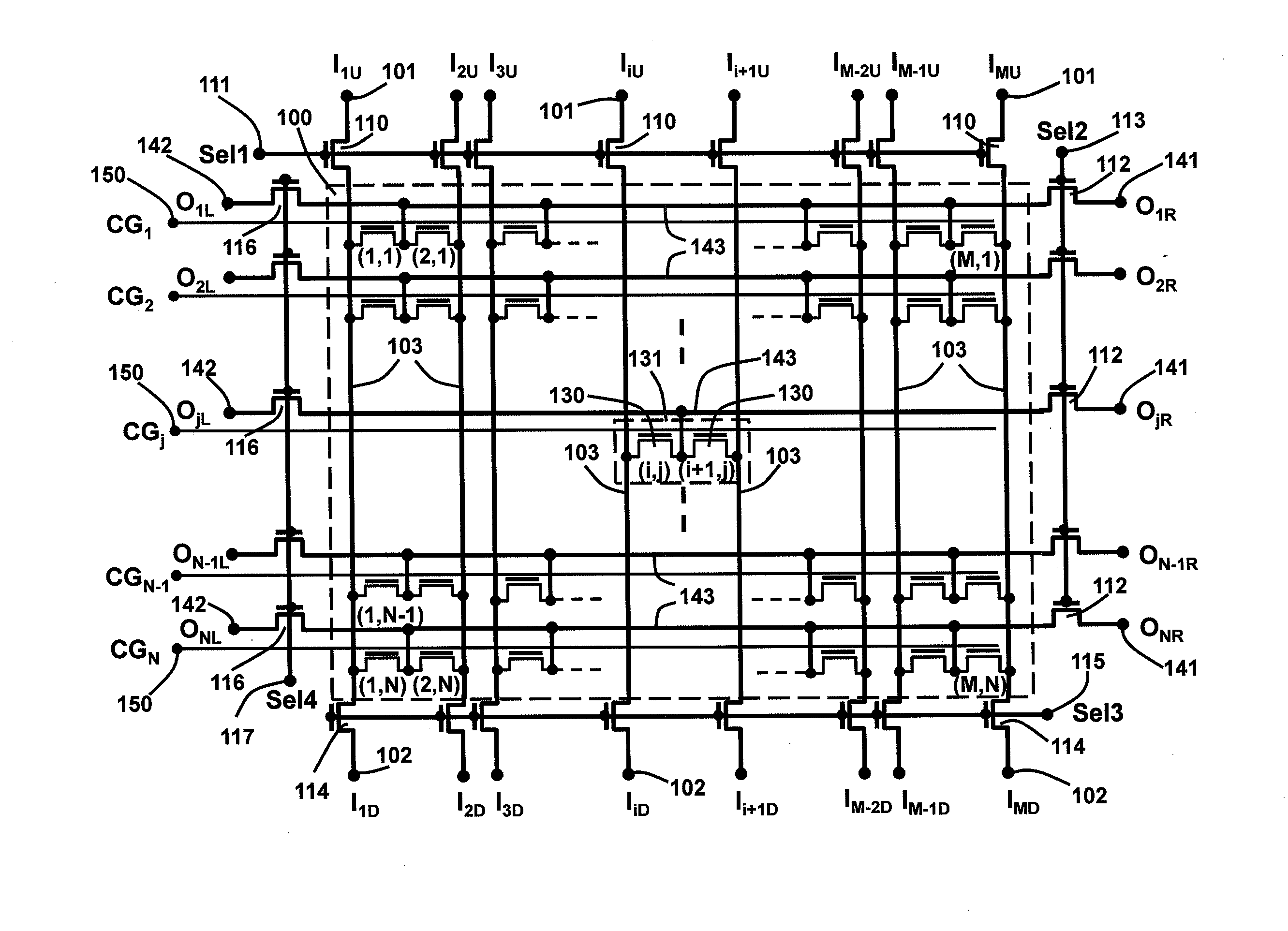
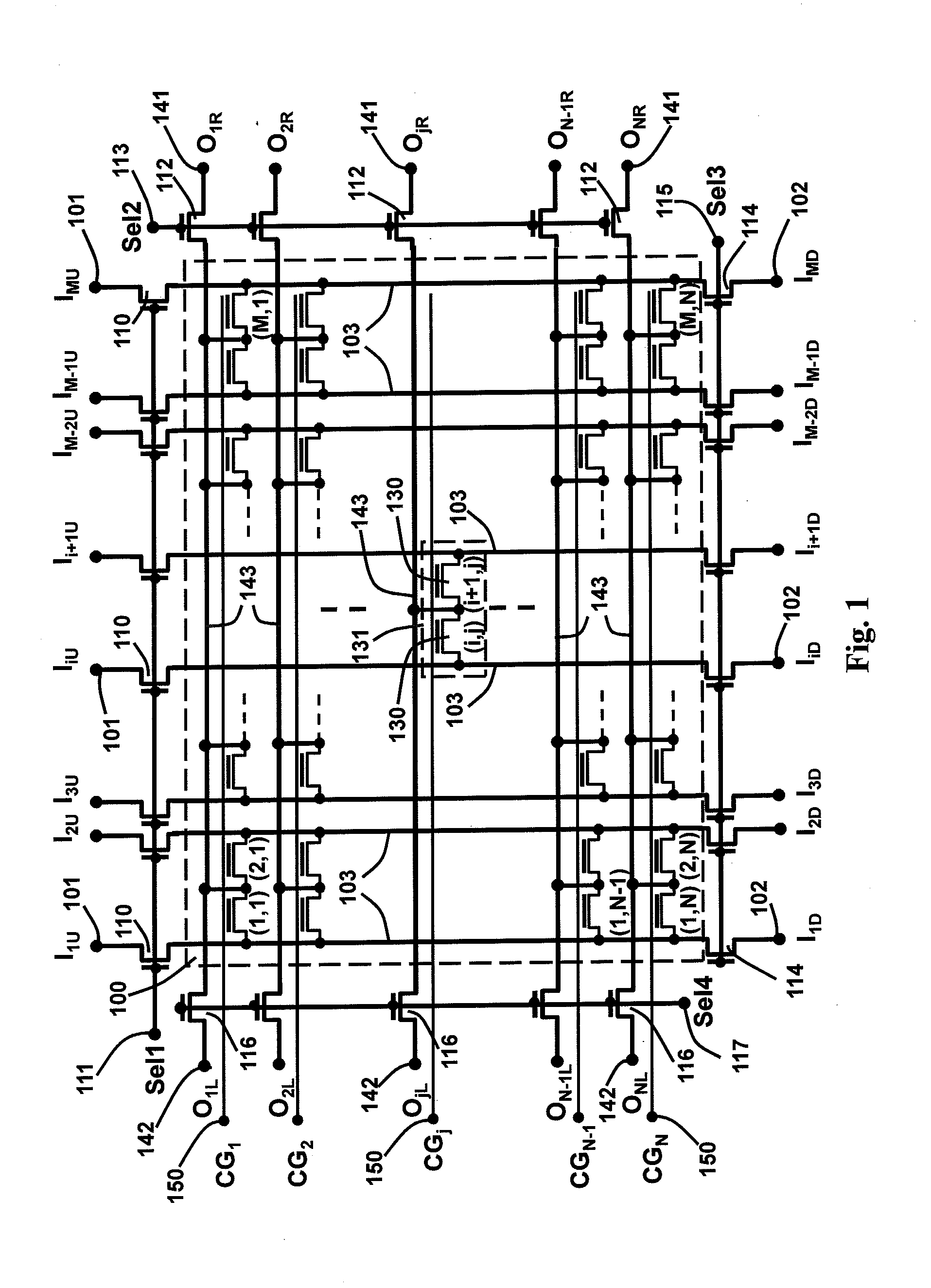
[0022]In the preferred embodiment, an M×N N-type SGLNVM array 100 in NOR configuration forms the M×N interconnection matrix as the schematic shown in FIG. 1. The N-type SGLNVM cell array 100 is fabricated by standard CMOS proces...


PUM


Abstract

An interconnection matrix consists of a plurality of semiconductor Non-Volatile Memory (NVM) forming an M×N array. Semiconductor NVM devices in the array are either programmed to a high threshold voltage state or erased to a low threshold voltage state according to a specific interconnection configuration. Applied with a gate voltage bias higher than the low threshold voltage and lower than the high threshold voltage to the control gates of the entire semiconductor NVM devices in the array, the configured interconnection network is formed. The disclosed interconnection matrix can be applied to configuring circuit routing in Integrated Circuit (IC).

Description

BACKGROUND OF THE INVENTION[0001]1. Field of the invention[0002]This invention relates to interconnection matrixes for circuit routing in Integrated Circuit (IC). In particular, an array of semiconductor NVM devices is applied to form an interconnection matrix. Applied with a control gate voltage bias lower than the high threshold voltage and higher than the low threshold voltage, the NVM devices with programmed high threshold voltages are “off” to disconnect the two input-output terminals. While the un-programmed NVM devices with low threshold voltages having the same applied control gate bias are “on” to connect the two input-output terminals.[0003]2. Description of the Related Art[0004]In field of Integrated Circuit (IC), active elements like transistors and passive elements like resistors and capacitors are connected by metal wires and inter-layered metal vias / contacts. The metal connection is usually done by the final metallization process in semiconductor manufacturing. Once t...

Claims


Application Information

Patent Timeline
Patent Type & Authority Applications(United States)
IPC IPC(8): G11C16/04
CPCG11C16/04G11C16/0441G11C16/0483G11C16/10G11C16/3418
Inventor WANG, LEE
Owner FLASHSILICON
Why Eureka
Try Eureka