
Gallium-nitride-on-diamond wafers and devices, and methods of manufacture
a technology of diamond wafers and diamonds, which is applied in the direction of crystal growth process, chemically reactive gas, polycrystalline material growth, etc., can solve the problems of unacceptably high bow and reduce the thermal resistance of any electronic and optoelectronic device, so as to improve the quality of the epilayer, improve the thermal resistance, and improve the effect of gan-on-diamond wafers
- Summary
- Abstract
- Description
- Claims
- Application Information
AI Technical Summary
Benefits of technology
Problems solved by technology
Method used
Image

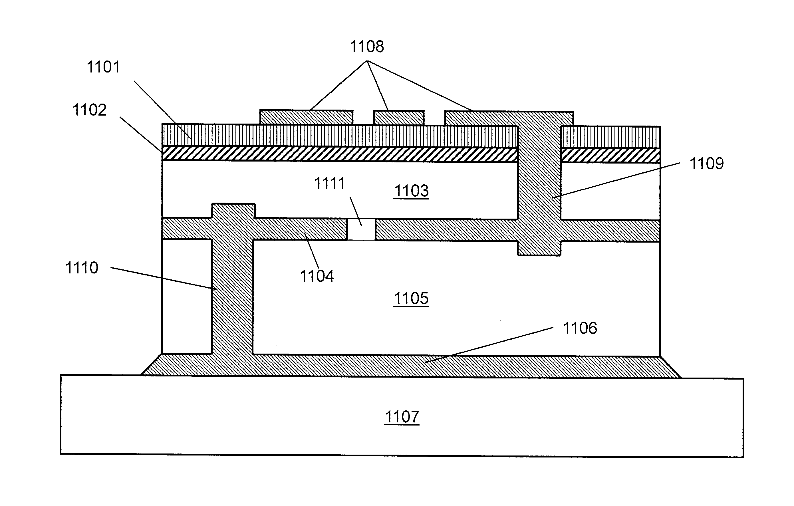
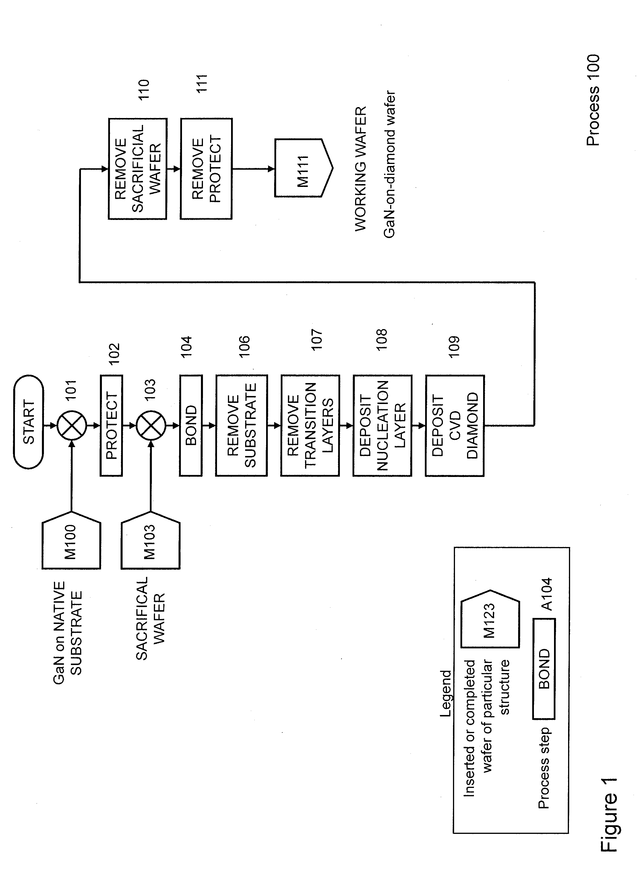
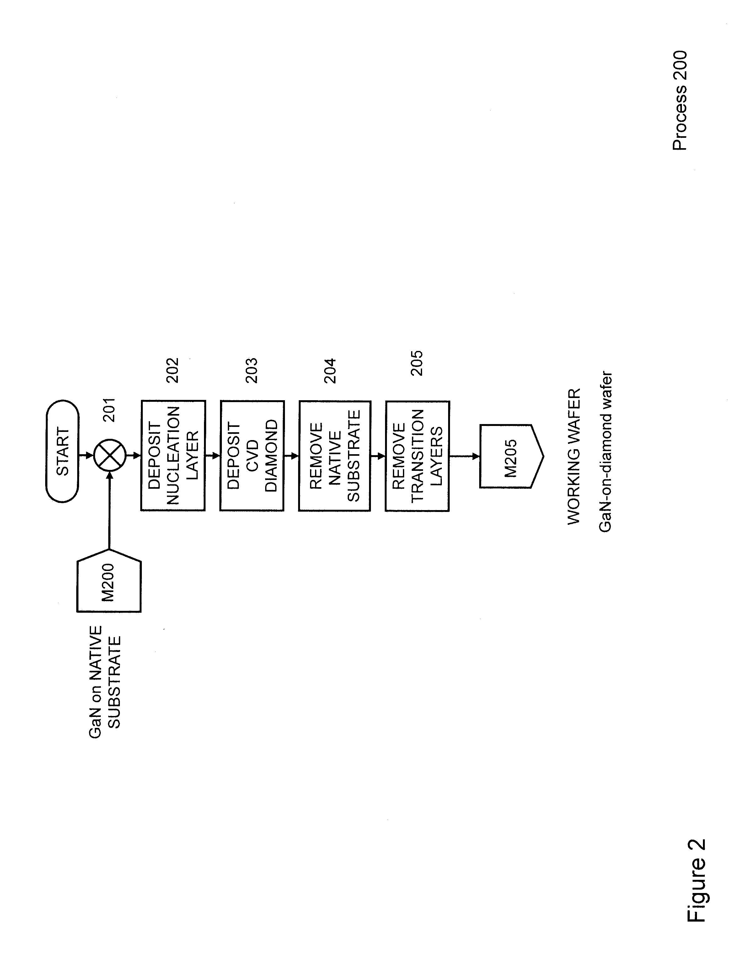
Examples
process embodiment
Detailed Wafer Structure and Process Embodiment Descriptions
[0107](a) 100-400-500. In one embodiment of preferred method for the manufacturing of high-quality GaN-on-diamond wafers and devices, an as-grown wafer M100 with preferred structure 700 is provided as input to the preferred method 100. The structure of the wafer resulting from process 100 may be, but is not limited to preferred wafer structure 750. The working wafer M111 resulting from process 100 is then provided as input wafer M400 to process 400. The structure of the wafer resulting from process 400 may be, but is not limited to preferred wafer structure 770. In another embodiment, the resulting composite wafer M405 is further processed into devices using process 500, resulting in chips M506 which may have, but are not limited to chip or wafer structure 780.
[0108](b) 100-600. In one embodiment of preferred method for the manufacturing of high-quality GaN-on-diamond wafers and devices, an as-grown wafer M100 with preferre...
PUM
| Property | Measurement | Unit |
|---|---|---|
| thickness | aaaaa | aaaaa |
| thickness | aaaaa | aaaaa |
| thickness | aaaaa | aaaaa |
Abstract
Description
Claims
Application Information