Display device

a display device and display technology, applied in the field of display devices, can solve the problems of reducing display quality and changing the voltage corresponding to a signal written into a pixel with time, and achieve the effect of high display quality

Inactive Publication Date: 2014-05-29
SEMICON ENERGY LAB CO LTD
View PDF32 Cites 43 Cited by
  • Summary
  • Abstract
  • Description
  • Claims
  • Application Information

AI Technical Summary

Benefits of technology

[0012]With one embodiment of the present invention, a novel display device with high display quality can be provided.

Problems solved by technology

However, a voltage corresponding to a signal written into a pixel changes with time.
Once the amount of change in voltage written into each pixel exceeds an amount corresponding to the allowable variation range of gray level in one image, a user perceives a flicker of the image, resulting in a reduction in display quality.

Method used


Image

  • Display device
  • Display device
  • Display device

Examples


embodiment 1

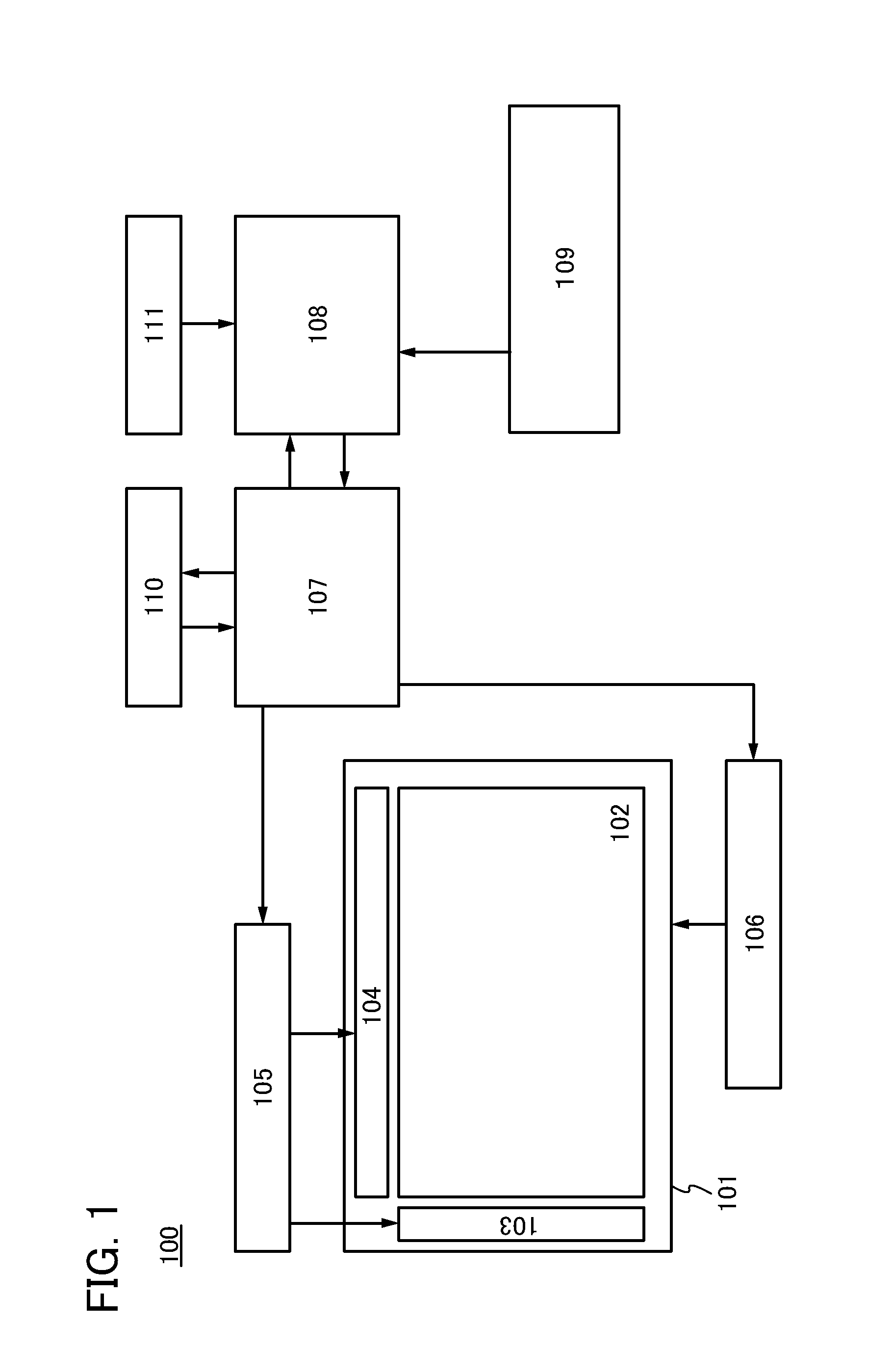
[0057]In Embodiment 1, an example of the structure of a display device in one embodiment of the present invention will be described with reference to FIG. 1, FIGS. 2A and 2B, FIG. 3, FIG. 4, and FIG. 5.

[0058]In this specification and the like, a display device includes display elements. Examples of display elements are liquid crystal elements (also referred to as liquid crystal display elements), light-emitting elements (also referred to as light-emitting display elements), electrophoretic elements, and electrowetting elements. A light-emitting element includes, in its category, an element whose luminance is controlled by current or voltage, and specifically includes an inorganic electroluminescent (EL) element and an organic EL element. Further, a display medium whose contrast is changed by an electric effect, such as electronic ink, can be used.

[0059]In addition, the display device includes, in its category, a panel in which a display element is sealed and a module in which an IC ...

embodiment 2

[0091]In Embodiment 2, an example of a method of driving the display device shown in Embodiment 1 will be described with reference to FIG. 1, FIGS. 2A and 2B, FIG. 6, and FIG. 7.

[0092]Specifically, the description is made on a method of switching between a first mode where a first driving signal (also referred to as G signal) for selecting a pixel is output at 60 Hz or more and a second mode where the G signal is output at 30 Hz or less, preferably 1 Hz or less, more preferably 0.2 Hz or less.

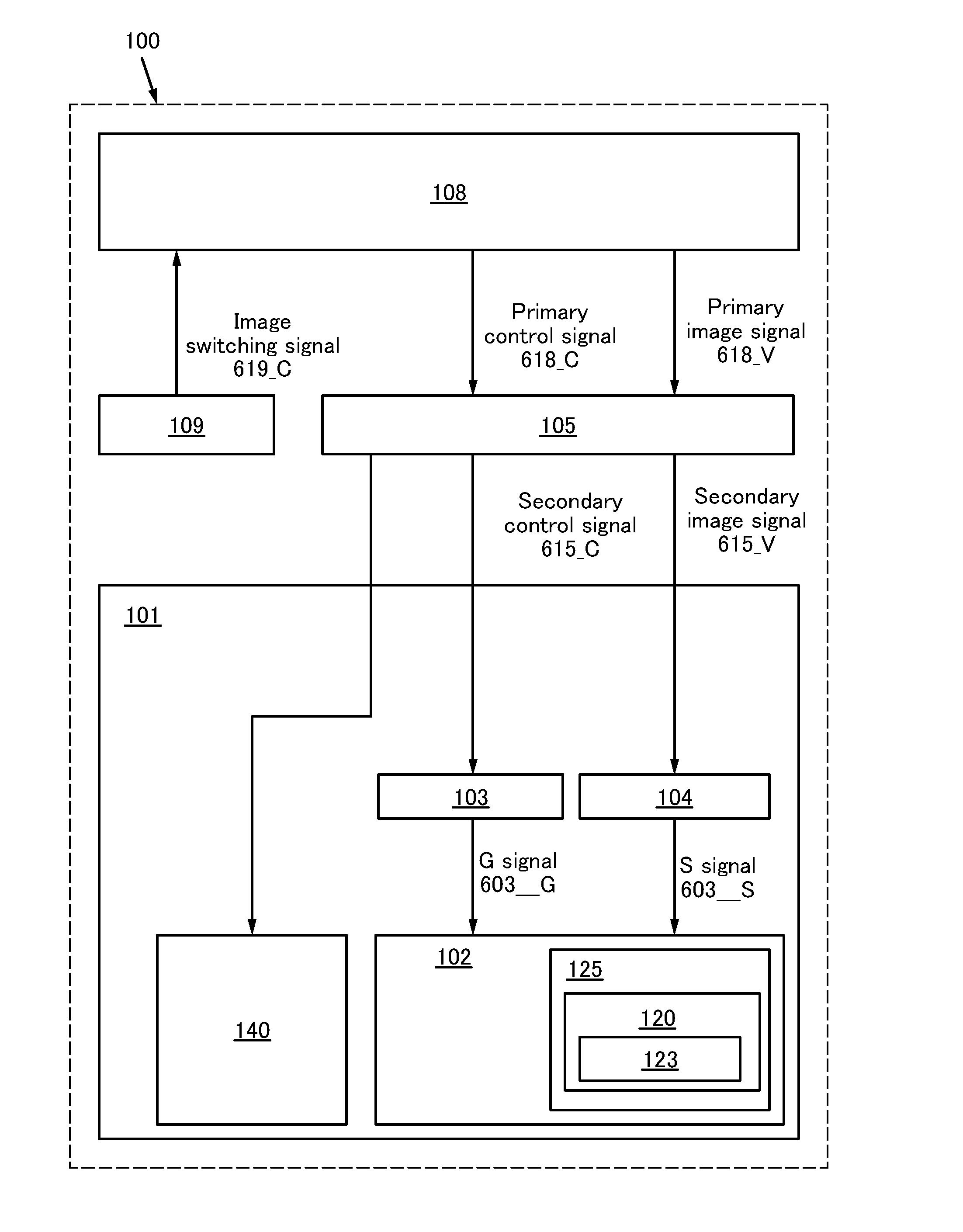
[0093]FIG. 6 is a block diagram of the display device 100 in FIG. 1, in which the control circuit 106, the image processing circuit 107, the memory device 110, and the temperature sensing unit 111 are not shown.

[0094]The arithmetic processing unit 108 generates a primary control signal 618_C and a primary image signal 618_V. The arithmetic processing unit 108 may generate the primary control signal 618_C including a mode switching signal in accordance with an image switching signal 619_C input ...

embodiment 3

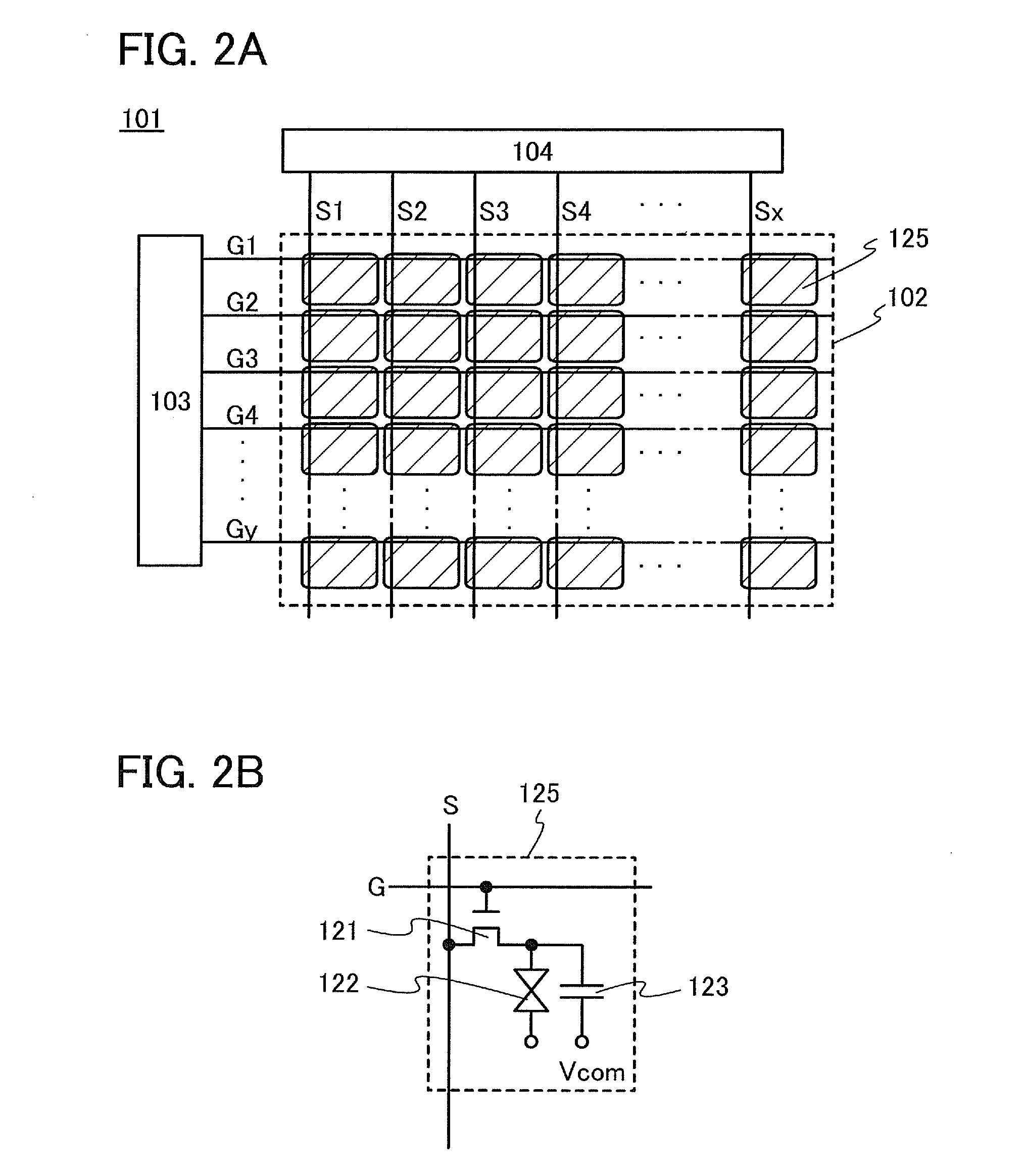
[0125]In Embodiment 3, another example of a method of driving the display device shown in Embodiment 1 will be described with reference to FIGS. 2A and 2B and FIG. 8.

[0126]An example of a method of writing the S signal 603_S into the pixel portion 102 illustrated in FIG. 2A will be described. Specifically, a method of writing the S signal 603_S into each pixel 125 in FIG. 2B of the pixel portion 102 will be described. Note that the description of FIG. 6 can be referred to for the details of the S signal and the G signal; therefore, the detailed description is not repeated in this embodiment.

[0127]In a first frame period, the pulsed G signal 603_G is input to the first wiring G1, so that the first wiring G1 is selected. In each of the plurality of pixels 125 connected to the selected first wiring G1, the transistor 121 is turned on.

[0128]When the transistors 121 are on (in one line period), the potential of the S signal 603_S generated from the secondary image signal 615_V is applied...


PUM


Abstract

To provide a novel display device without deterioration of display quality, the display device includes a display panel including a pixel portion that displays still images at a frame frequency of 30 Hz or less, a temperature sensing unit that senses the temperature of the display panel, a memory device that stores a correction table containing correction data, and a control circuit to which correction data selected from the correction table is input in accordance with an output of the temperature sensing unit. The pixel portion includes a plurality of pixels. Each of the pixels includes a transistor, a display element, and a capacitor. The control circuit outputs a voltage based on the correction data input to the control circuit, to the capacitor included in each of the pixels.

Description

TECHNICAL FIELD[0001]The present invention relates to an object, a method, a manufacturing method, a process, a machine, manufacture, or composition of matter. In particular, the present invention relates to, for example, a semiconductor device, a display device, a light-emitting device, a driving method thereof, or a manufacturing method thereof. The present invention particularly relates to, for example, a semiconductor device including an oxide semiconductor, a display device including an oxide semiconductor, or a light-emitting device including an oxide semiconductor.BACKGROUND ART[0002]The information revolution has progressed rapidly with technological innovation, mainly with innovation in information processing, and the variety of uses of displays, for example, for personal computers and mobile devices has increased at workplaces and homes. Accordingly, the frequency and time of use of displays have increased dramatically.[0003]There have been demands for higher resolution an...

Claims


Application Information

Patent Timeline
Patent Type & Authority Applications(United States)
IPC IPC(8): G09G5/00G09G3/36
CPCG09G3/3648G09G5/00G09G3/3655G09G3/3696G09G2320/041G09G2320/103G09G2340/0435
Inventor KOYAMA, JUNMIYAKE, HIROYUKI
Owner SEMICON ENERGY LAB CO LTD
Why Eureka
Try Eureka