Method for forming laminate

a technology of laminates and substrates, applied in the direction of solid-state devices, layered products, chemistry apparatus and processes, etc., can solve the problems of difficult temporary adhesion technology and difficulty in separating the support plate from the wafer substra

Inactive Publication Date: 2014-06-05
TOKYO OHKA KOGYO CO LTD
View PDF3 Cites 23 Cited by
  • Summary
  • Abstract
  • Description
  • Claims
  • Application Information

AI Technical Summary

Benefits of technology

[0018]When the laminate is subjected to a desired treatment, the method for forming a laminate according to the present invention gives rise to an effect for one to adequately protect the release layer by the protective layer.

Problems solved by technology

In the case of firmly adhering the wafer substrate and the support plate to each other, it is difficult to separate the support plate from the wafer substrate without damaging the structures mounted on the wafer substrate depending upon an adhesive material.
In consequence, the development of a very difficult temporary adhesion technology for realizing firm adhesion between the wafer substrate and the support plate during the manufacturing process and meanwhile separating an element mounted on the wafer substrate without being damaged after the manufacturing process is demanded.

Method used


Image

  • Method for forming laminate
  • Method for forming laminate
  • Method for forming laminate

Examples


embodiments

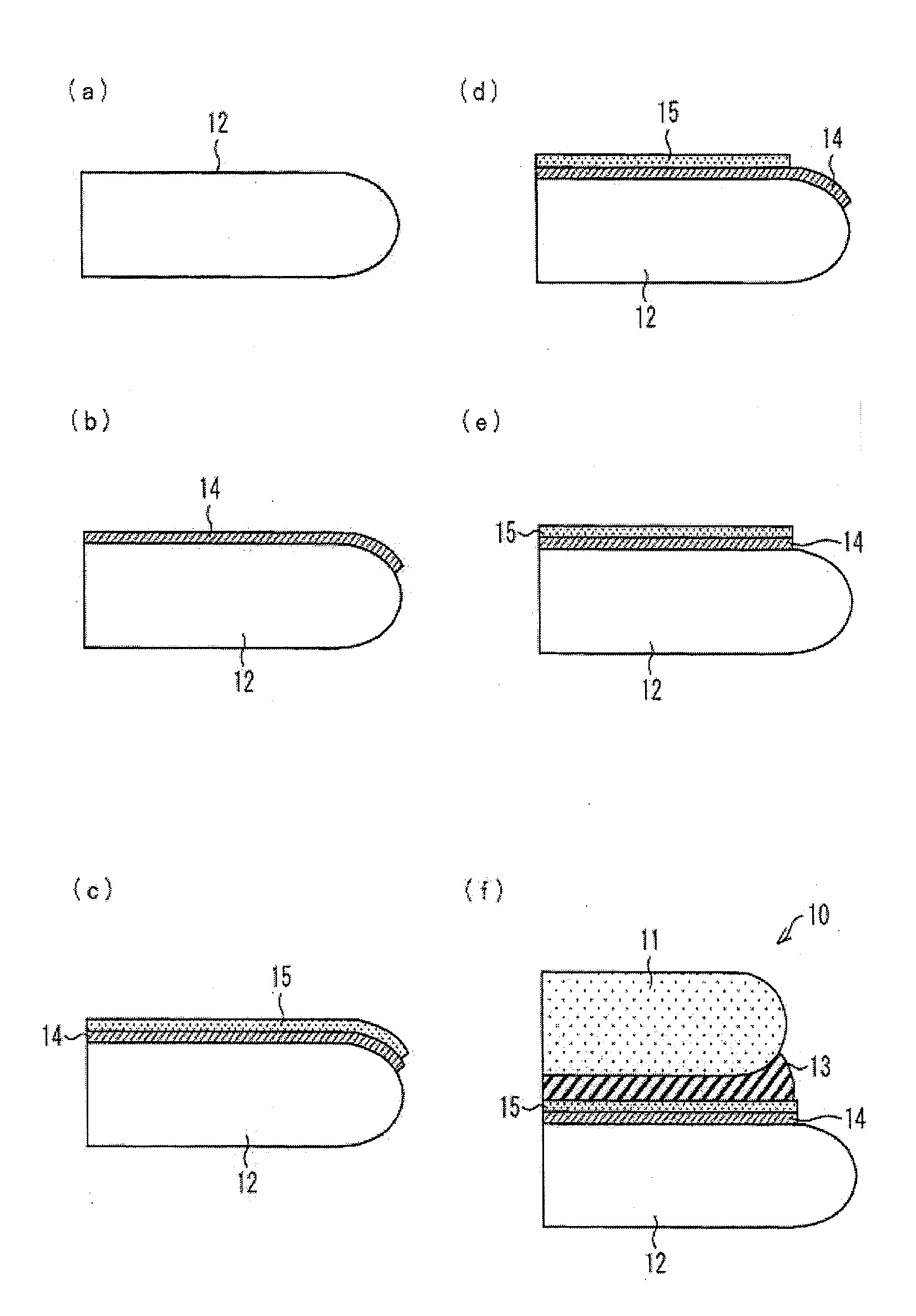
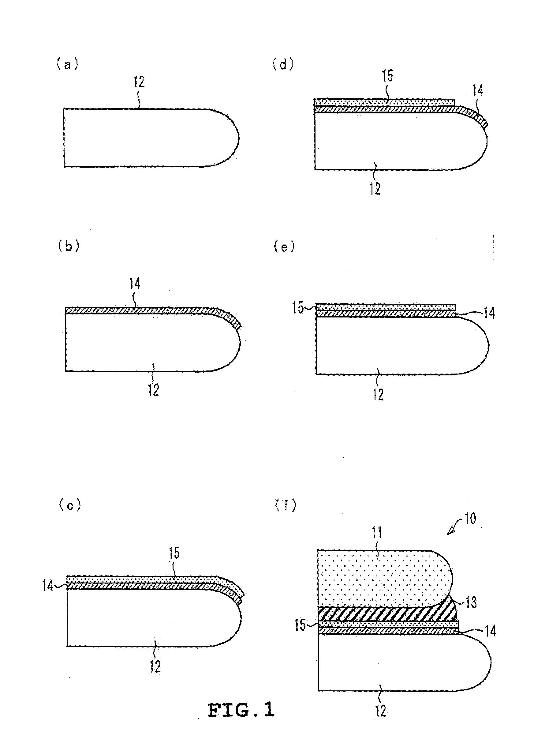
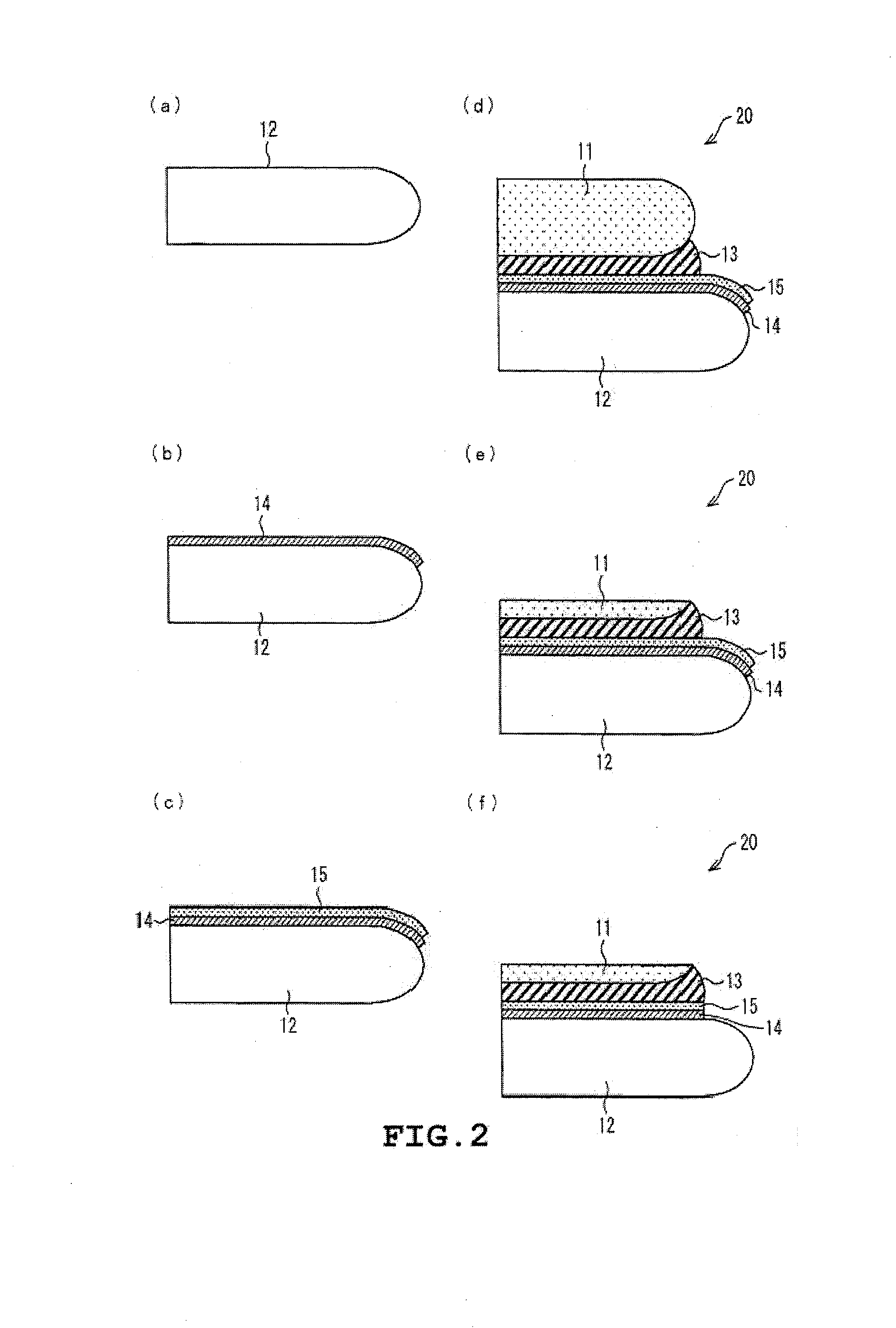
[0029]An embodiment of the present invention is hereunder described in detail. According to the present embodiment, a laminate 10 is formed as illustrated in FIG. 1(f).

[0030]A method for forming a laminate 10 according to the present embodiment is concerned with a method for forming a laminate 10 comprising laminating a substrate 11, an adhesive layer 13, a release layer 14 which is denatured upon absorption of light, and a support plate (support) 12 supporting the substrate 11 in this order to form the laminate 10, the method including a protective layer forming step of forming a protective layer 15 for covering a face that is a surface of the release layer 14 and which is not adhered to the support plate 12 and not superimposed at least on the adhesive layer 13; and a protective layer removal step of removing a portion of the protective layer 15, which is exposed at the time of forming the laminate 10. First of all, each of the constitutions forming the laminate 10 is hereunder de...

example 1

Formation of Laminate

[0186](Process)

[0187]A fluorocarbon film (thickness: 1 μm) that is a release layer was formed on a support (12-inch glass substrate, thickness: 700 μm) under conditions of a flow rate of 400 sccm, a pressure of 700 mTorr, a high-frequency electric power of 2,500 W, and a deposition temperature of 240° C. by a CVD method using C4F8 as a reaction gas, and TZNR-A3007t (manufactured by Tokyo Ohka Kogyo Co., Ltd.) that is an adhesive composition was applied thereonto, followed by baking at 220° C. for 3 minutes, thereby forming a protective layer having a film thickness of 1.5 μm (protective layer forming step). The above-described adhesive composition containing 280 parts by weight of a prime solvent was spin-applied on a 12-inch silicon wafer and heated at 100° C., 160° C. and 200° C. for 3 minutes each, to form an adhesive layer (film thickness: 50 μm), which was then stuck to a glass support in vacuo under conditions of 220° C. and 4,000 kg for 3 minutes, thereby...

example 2

Formation of Laminate

[0192]A laminate was formed under the same conditions as those in Example 1. The laminate formed in this Example is different from the laminate formed in Example 1 at the point that the protective layer is not formed.

Removal of Release Layer by Plasma Treatment

[0193]Subsequently, the release layer of a portion exposed from the wafer which had been stuck to the support plate via the adhesive layer was removed by a plasma treatment. The plasma treatment was conducted using an interdigitated array electrode or an ICP electrode under the following conditions.

[0194]The plasma treatment in the case of using an interdigitated array electrode was conducted under conditions of a power of 1,200 W, a pressure of 0.5 Torr, a gas flow rate of 1,200 sccm (O2), a stage temperature of 90° C., and a treatment time by holding by pinning up of 3 minutes. The plasma treatment in the case of using an ICP electrode was conducted under conditions of a power of 600 W, a pressure of 130...


PUM

PropertyMeasurementUnit
thicknessaaaaaaaaaa
thicknessaaaaaaaaaa
thicknessaaaaaaaaaa

Abstract

A release layer is adequately protected by a protective layer when a laminate is subjected to a desired treatment. A method for forming a laminate 10 includes a protective layer forming step of forming a protective layer 15 for covering a face that is a surface of a release layer 14 and which is not adhered to a support plate 12 and not superimposed at least on an adhesive layer 13; and a protective layer removal step of removing a portion of the protective layer 15, which is exposed at the time of forming the laminate 10.

Description

CROSS-REFERENCE TO RELATED APPLICATIONS[0001]Priority is claimed on Japanese Patent Application No. 2012-266699, filed Dec. 5, 2012, the content of which is incorporated herein by reference.TECHNICAL FIELD[0002]The present invention relates to a method for forming a laminate.BACKGROUND ART[0003]In recent years, thinning, downsizing, weight reduction, and the like of electronic appliances such as IC cards and mobile phones are required. In order to meet these requirements, a thinned semiconductor chip must be used even for semiconductor chips which are installed. For that reason, although a thickness (film thickness) of a wafer substrate which is a basis of the semiconductor chip is 125 μm to 150 lam in the existing circumstances, it is said that the thickness must be reduced to an extent of 25 μm to 50 μm for chips of the next generation. In consequence, in order to obtain a wafer substrate having the above-described film thickness, a thinning step of the wafer substrate is necessar...

Claims


Application Information

Patent Timeline
Patent Type & Authority Applications(United States)
IPC IPC(8): H01L21/683
CPCH01L21/6836H01L21/6835H01L2221/68318H01L2221/68327H01L2221/6834H01L2221/68381H01L21/20
Inventor MIYANARI, ATSUSHINAKAMURA, AKIHIKO
Owner TOKYO OHKA KOGYO CO LTD
Why Eureka
Try Eureka