Hybrid nanomesh structures

a technology of hybrid materials and nanomesh, applied in the field of hybrid nanomesh structures, can solve the problems of difficult integration of p n-type field effect transistors employing different semiconductor materials onto the same substrate in random patterns, and achieve the effect of challenging the challenge even mor

Inactive Publication Date: 2014-06-05
GLOBALFOUNDRIES INC
View PDF6 Cites 59 Cited by
  • Summary
  • Abstract
  • Description
  • Claims
  • Application Information

AI Technical Summary

Problems solved by technology

However, integration of p-type field effect transistors and n-type field effect transistors employing different semiconductor materials onto a same substrate in a random pattern is a difficult challenge because two types of semiconductor materials need to be provided in an arbitrary pattern as needed by a circuit layout.
This challenge becomes even more difficult when fabrication of three dimensional structures is attempted, which is desirable for the purpose of improving electrostatic control of the gate over the channel and for increasing layout density by decreasing the FET channel footprint.

Method used


Image

  • Hybrid nanomesh structures
  • Hybrid nanomesh structures
  • Hybrid nanomesh structures

Examples


Embodiment Construction

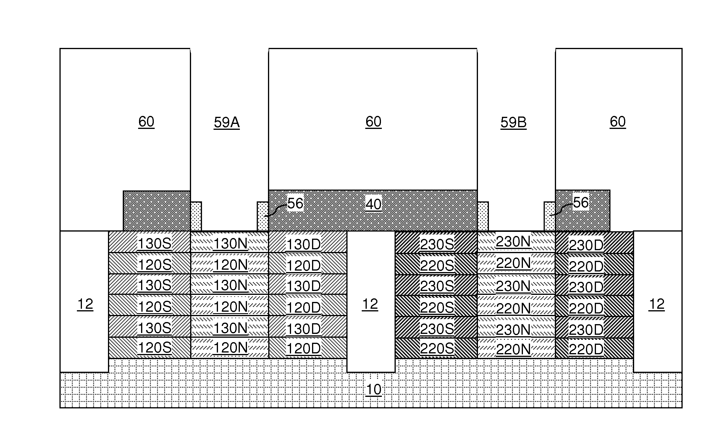
[0042]As stated above, the present disclosure relates to hybrid nanomesh structures and a method of manufacturing the same. Aspects of the present disclosure are now described in detail with accompanying figures. It is noted that like reference numerals refer to like elements across different embodiments. The drawings are not necessarily drawn to scale.

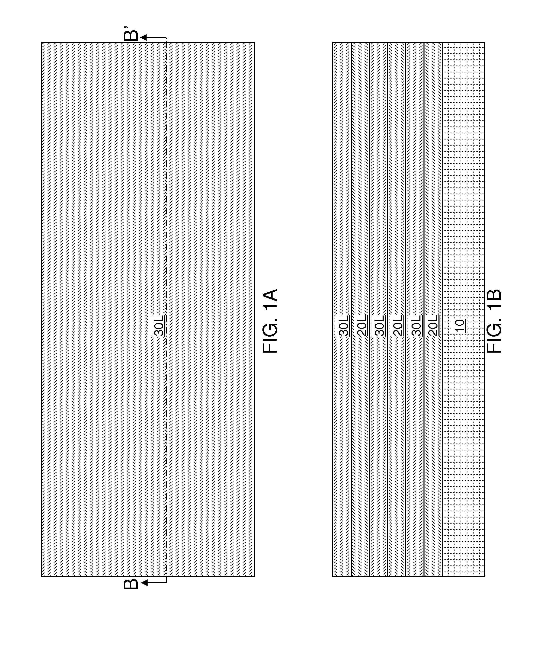
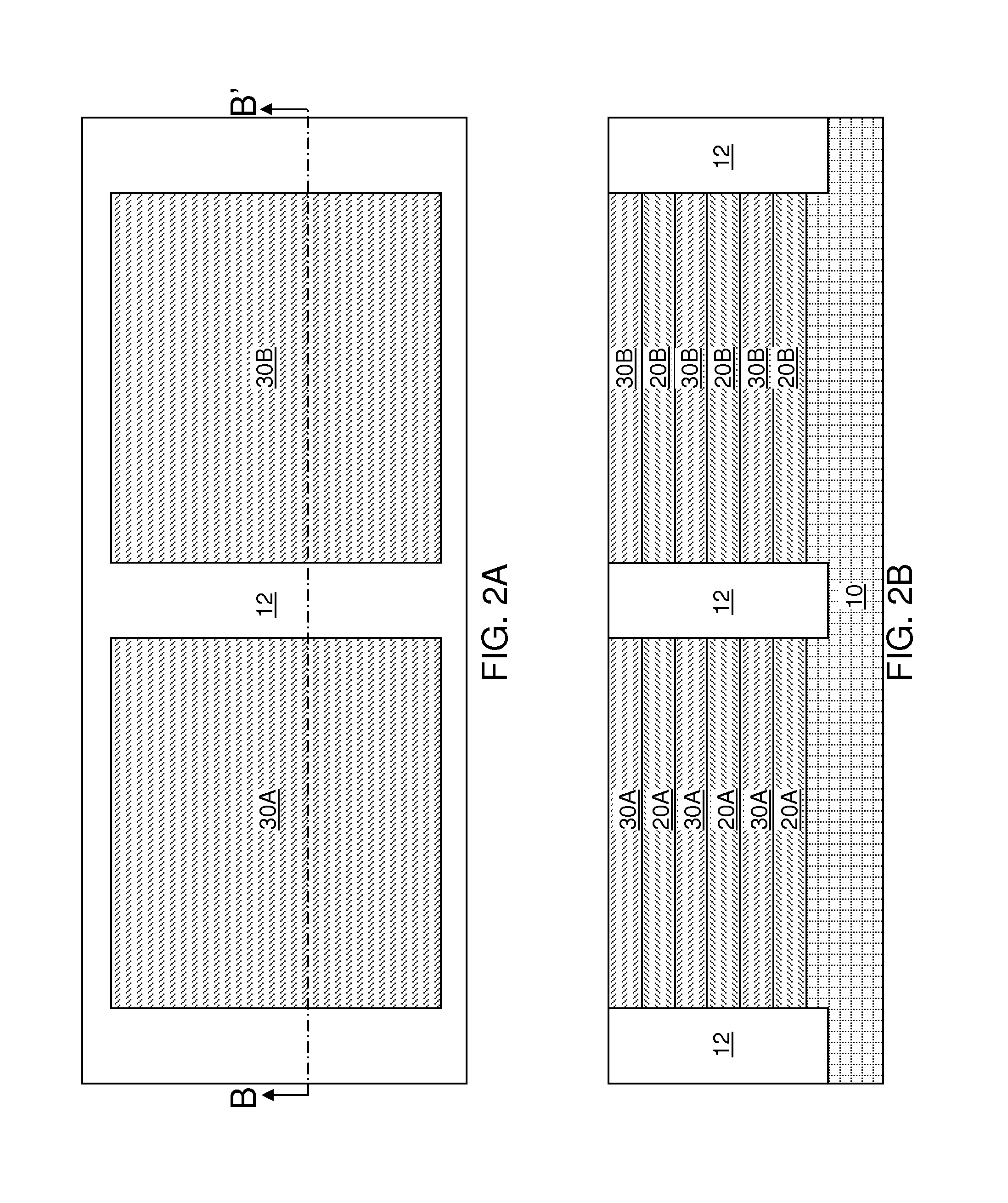
[0043]Referring to FIGS. 1A and 1B, an exemplary semiconductor structure according to an embodiment of the present disclosure includes a single crystalline substrate layer 10 and an alternating stack of a first semiconductor material and a second semiconductor material. The single crystalline substrate layer 10 includes a single crystalline semiconductor material. The single crystalline semiconductor material of the single crystalline substrate layer 10 can be a III-V compound semiconductor material or an elemental semiconductor material or an alloy of at least two elemental semiconductors. Exemplary III-V compound semiconductor mater...


PUM


Abstract

An alternating stack of first and second semiconductor layers is formed. Fin-defining mask structures are formed over the alternating stack. A planarization dielectric layer and first and second gate cavities therein are subsequently formed. The first and second gate cavities are extended downward by etching the alternating stack employing a combination of the planarization layer and the fin-defining mask structures as an etch mask. The second semiconductor material is isotropically etched to laterally expand the first gate cavity and to form a first array of semiconductor nanowires including the first semiconductor material, and the first semiconductor material is isotropically etched to laterally expand the second gate cavity and to form a second array of semiconductor nanowires including the second semiconductor material. The first and second gate cavities are filled with replacement gate structures. Each replacement gate structure laterally can surround a two-dimensional array of semiconductor nanowires.

Description

RELATED APPLICATIONS[0001]The present application is related to co-assigned and co-pending U.S. application Ser. No. ______ (Attorney Docket No: YOR920120671US1; SSMP 29136), which is incorporated herein by reference.BACKGROUND[0002]The present disclosure relates to a semiconductor structure, and particularly to hybrid nanomesh structures and a method of manufacturing the same.[0003]Semiconductor materials that provide optimal performance for p-type field effect transistors are different from semiconductor materials that provide optimal performance for n-type field effect transistors. However, integration of p-type field effect transistors and n-type field effect transistors employing different semiconductor materials onto a same substrate in a random pattern is a difficult challenge because two types of semiconductor materials need to be provided in an arbitrary pattern as needed by a circuit layout. This challenge becomes even more difficult when fabrication of three dimensional s...

Claims


Application Information

Patent Timeline
Patent Type & Authority Applications(United States)
IPC IPC(8): H01L27/088H01L21/8232
CPCH01L21/8232H01L27/088B82Y10/00B82Y40/00H01L21/823807H01L27/092H01L29/0673H01L29/42376H01L29/42392H01L29/66469H01L29/775H01L29/78696Y10S977/762
Inventor CHANG, JOSEPHINE B.CHANG, PAULMAJUMDAR, AMLANSLEIGHT, JEFFREY W.
Owner GLOBALFOUNDRIES INC
Why Eureka
Try Eureka