Semiconductor device and method of manufacturing the same

Active Publication Date: 2014-06-12
AMKOR TECH JAPAN INC
View PDF2 Cites 0 Cited by
  • Summary
  • Abstract
  • Description
  • Claims
  • Application Information

AI Technical Summary

Benefits of technology

[0010]The present invention was arrived at in view of the problems described above and aims to provide a semiconductor device with excellent thermal resistance in which low thermal resistance and high density are simultaneously achieved and a meth

Problems solved by technology

Although a semiconductor device is known as is described in Japanese Laid Open Patent 2012-94592 for example as a package in which the upper surface of a heat sink is completely exposed, since warping is produced when the thermal expans

Method used


Image

  • Semiconductor device and method of manufacturing the same
  • Semiconductor device and method of manufacturing the same
  • Semiconductor device and method of manufacturing the same

Examples


Embodiment Construction

[0025]The embodiments of the present invention are explained below while referring to the drawings. Furthermore, the same reference symbols are attached to the same structural components and therefore repeating explanations between embodiments are omitted.

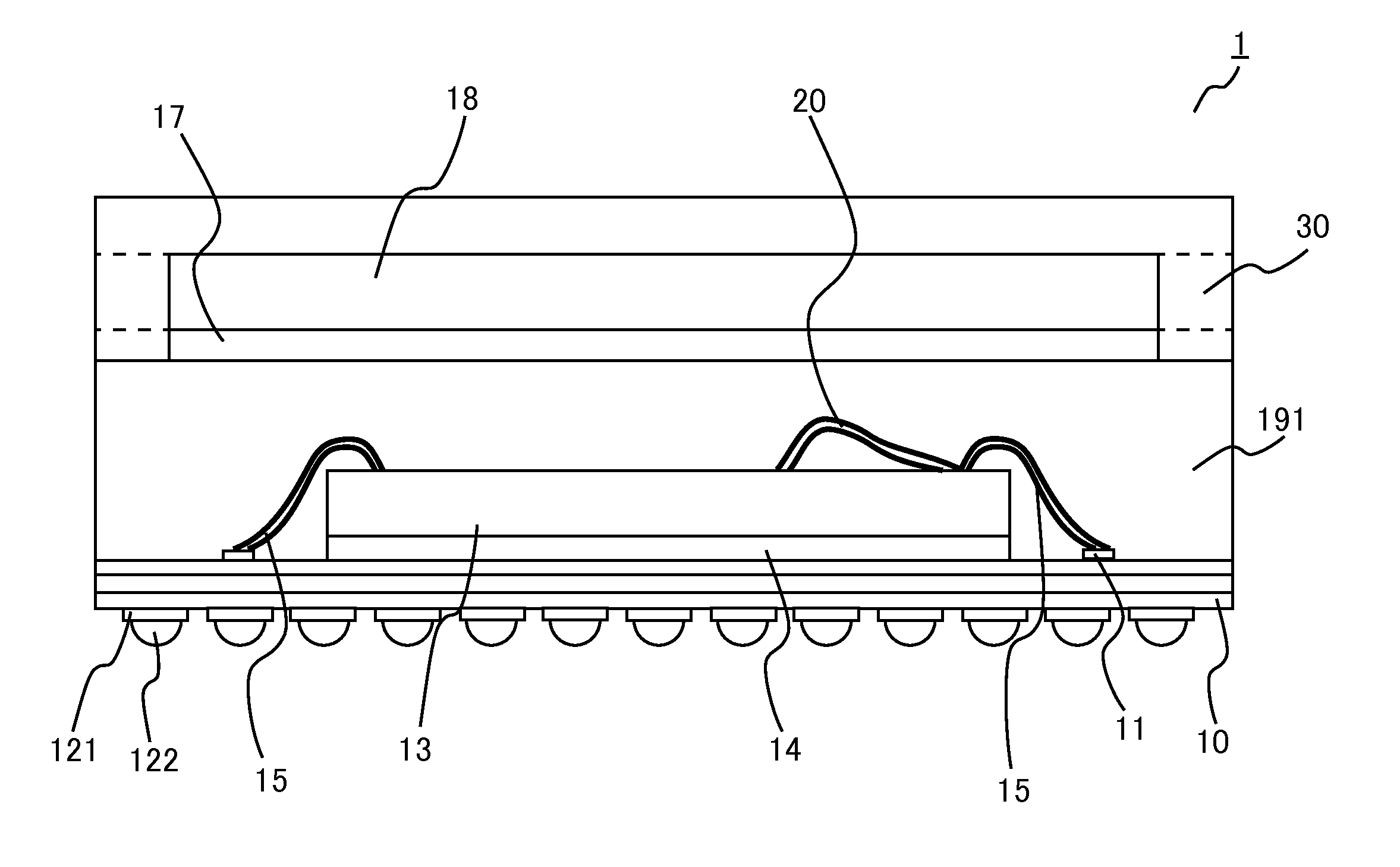
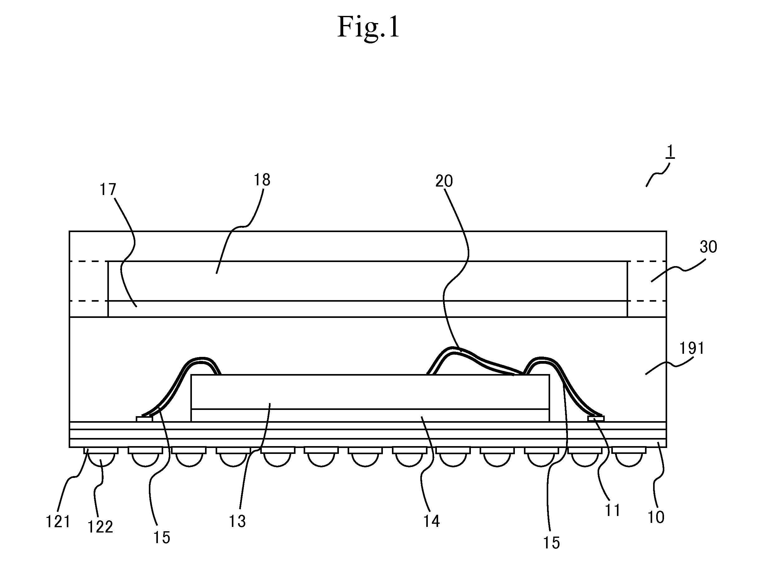
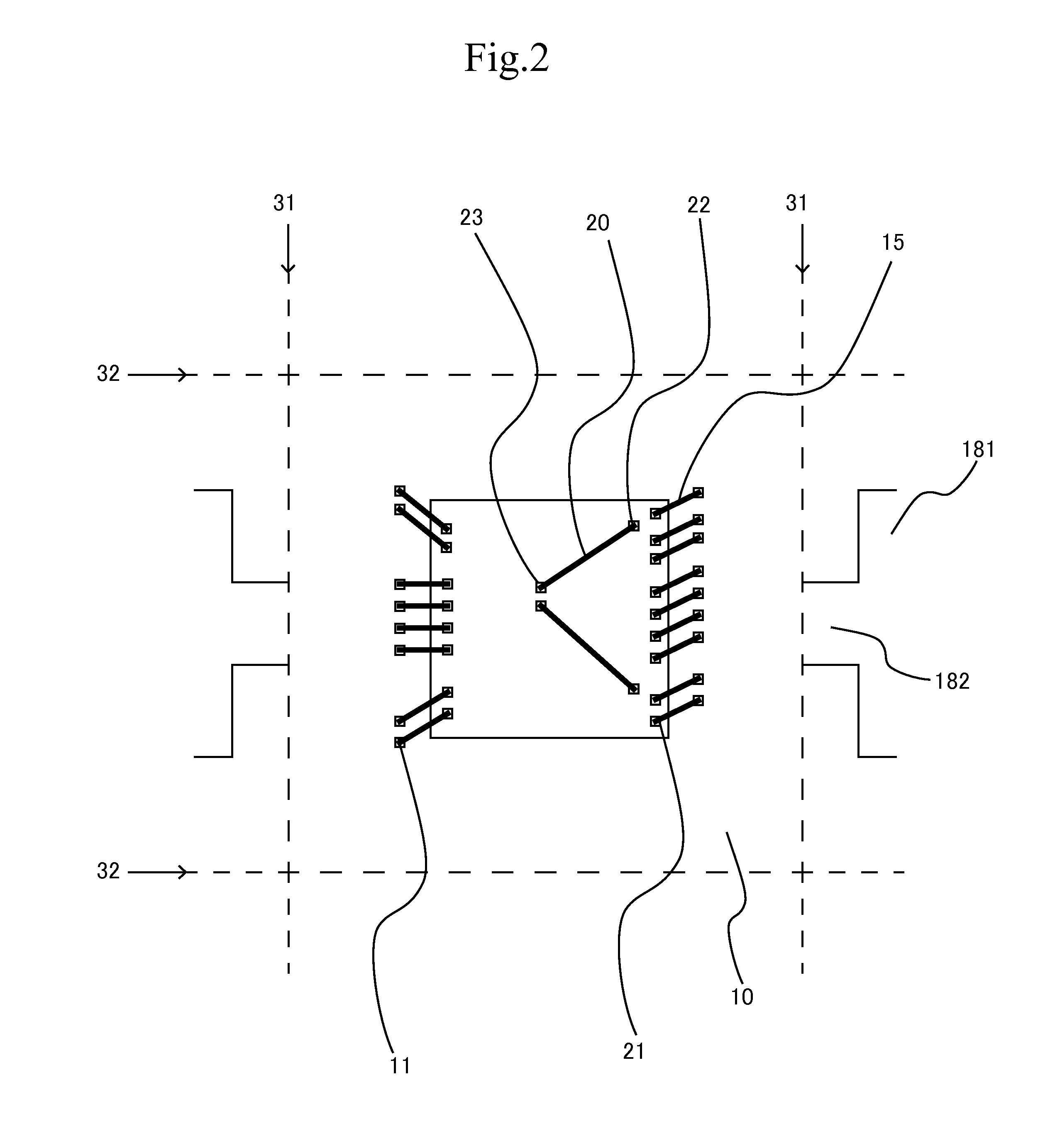
[0026]FIG. 1 is a cross-sectional diagram of a semiconductor device 1 which is a BGA package of one embodiment of the present invention. FIG. 2 is a planar view diagram of the semiconductor 1 which is a BGA package of one embodiment of the present invention (however, prior to formation of a sealing layer 30). The

[0027]BGA package is comprised from a substrate 10 (interposer), a semiconductor chip 13 mounted to the substrate 10 by an adhesive 14, a bonding wire 15 and bonding wire 20 connecting between the bonding pads, and a sealing layer 191 which seals these components using a sealing material. Furthermore, the package also includes a heat sink 18 mounted to the surface of the sealing layer 191 by an adhesive 17 and a sealing lay...


PUM


Abstract

A semiconductor device having a substrate including a plurality of external terminals on a rear surface and a plurality of bonding terminals electrically connected to the plurality of external terminals on a front surface, a semiconductor chip mounted on the front surface of the substrate, a surface of the chip including a plurality of bonding pads, a plurality of bonding wires connecting between the plurality of bonding pads or between the plurality of bonding terminals and the plurality of bonding wires respectively, a first sealing layer sealing the front surface of the substrate, the plurality of bonding wires and the semiconductor chip, and a second sealing layer comprised of the same material as the first sealing, the second sealing layer being formed above the first sealing layer.

Description

CROSS REFERENCE TO RELATED APPLICATION[0001]This application is based upon and claims the benefit of priority from the prior Japanese Patent Application No. 2012-267892, filed on Dec. 7, 2012; the entire contents of which are incorporated herein by reference.FIELD OF THE INVENTION[0002]The present invention is related to a semiconductor device and a method of manufacturing the same. In particular, the present invention is related to a semiconductor package in which a large heat generating semiconductor chip is sealed which simultaneously achieves low thermal resistance and high density and a method of manufacturing the same.BACKGROUND OF THE INVENTION[0003]A package is conventionally known which is installed with a heat sink as a package for use in relatively large heat generating semiconductor chip such as a graphics processor. Although a semiconductor device is known as is described in Japanese Laid Open Patent 2012-94592 for example as a package in which the upper surface of a he...

Claims


Application Information

Patent Timeline
IPC IPC(8): H01L23/495H01L21/56
CPCH01L21/56H01L23/49568H01L23/3128H01L23/3135H01L23/4334H01L21/565H01L24/48H01L2224/4813H01L2224/32225H01L2224/48227H01L2224/73265H01L2924/15311H01L24/45H01L2224/45144H01L2224/45147H01L24/29H01L24/32H01L24/49H01L24/73H01L2224/2919H01L2224/49175H01L2224/73215H01L2924/181H01L2224/05554H01L2924/10162H01L2924/00014H01L2924/00012H01L2924/00H01L2224/85399H01L2224/05599H01L23/34H01L23/28
Inventor TOMONAGA, YOSHIYUKIOOIDA, MITSURUWATANABE, KATSUMISATO, HIDENARI
Owner AMKOR TECH JAPAN INC
Why Eureka
Try Eureka