

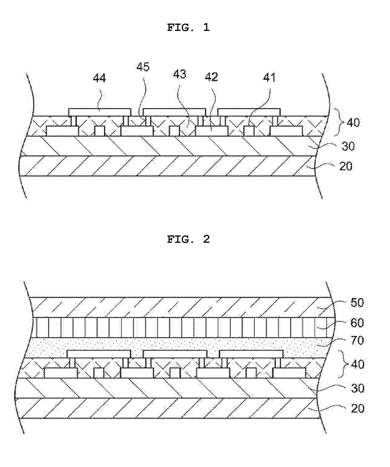
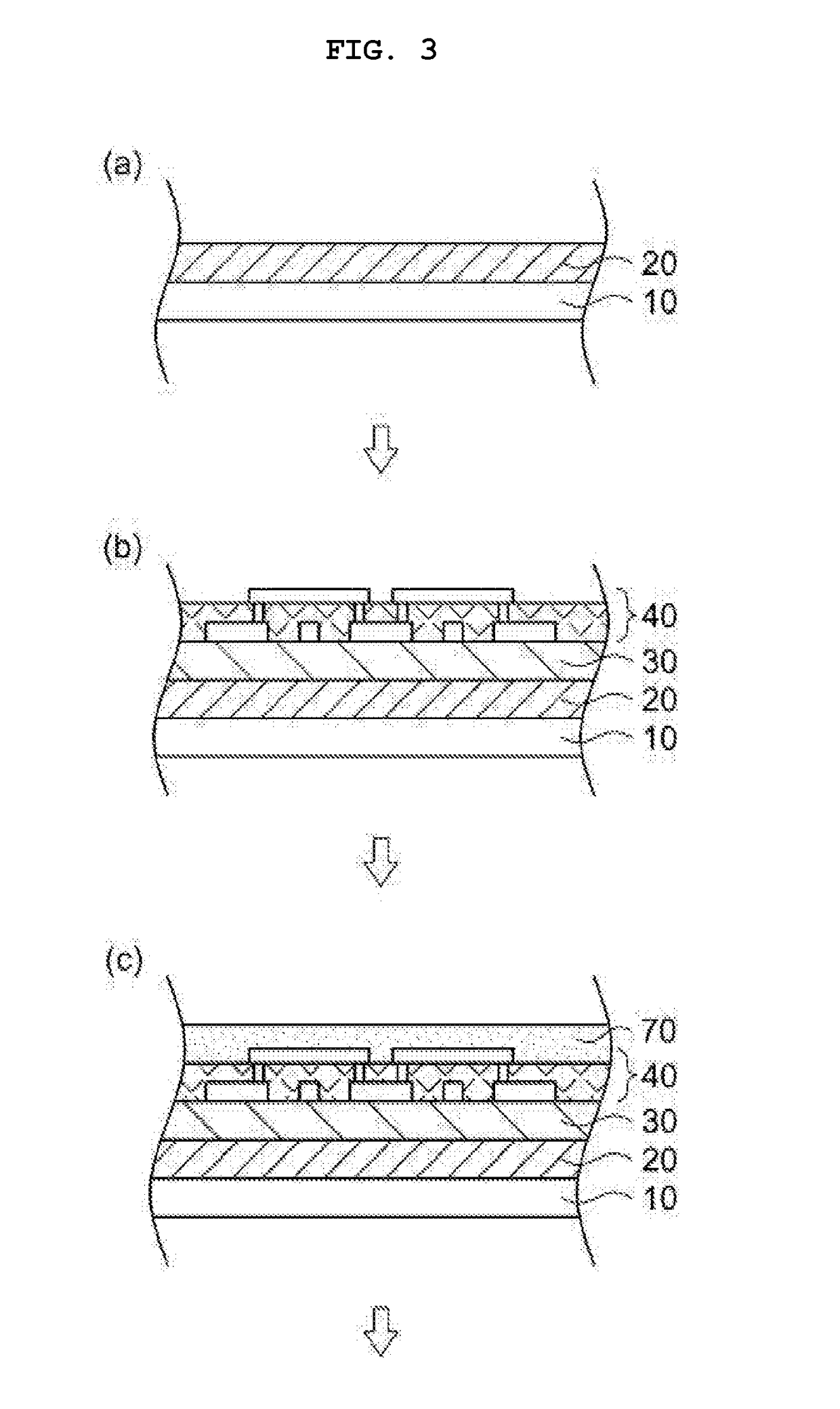
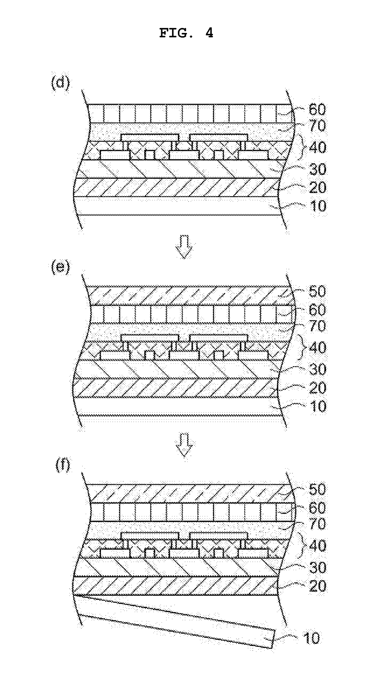
Film touch sensor and method for fabricating the same
- Summary
- Abstract
- Description
- Claims
- Application Information
AI Technical Summary
Benefits of technology
Problems solved by technology
Method used
Image

Examples
experimental example
[0254]1. Measurement of Sensitivity
[0255]Photosensitive resin compositions of the examples and comparative examples were applied to a glass substrate having a thickness of 0.7 mm (Corning 1737, manufactured by Corning Co.) with a spinner, and heated on a hot plate at 100° C. for 125 seconds to volatilize the solvent, thereby forming a photosensitive resin composition layer having a thickness of 4.0 μm.
[0256]Thereafter, in order to obtain a contact hole pattern having a diameter of 10 μm, exposure was performed with an i-beam stepper (NSR-205i11D, Nikon Co.) using a mask having a rectangular pattern opening whose exposed portion has sides of 10 μm.
[0257]The substrate after the exposure was subjected to a puddle development at 23° C. for 40 seconds using a 2.38% tetramethyl ammonium hydroxide aqueous solution as a developing solution, and then heated in an oven at 230° C. for 30 minutes to obtain a cured film.
[0258]Subsequently, the substrate was cut vertically, and an exposure amount...
PUM
| Property | Measurement | Unit |
|---|---|---|
| Temperature | aaaaa | aaaaa |
| Temperature | aaaaa | aaaaa |
| Time | aaaaa | aaaaa |
Abstract
Description
Claims
Application Information