
Organic light emitting display device and method for driving thereof

a technology of light-emitting display device and which is applied in the direction of instruments, static indicating devices, etc., can solve the problems of deteriorating luminance characteristics, lowering luminance and luminance deviation of organic light-emitting display device according to the related art, etc., and achieves the effect of facilitating luminance lowering and luminance deviation

Active Publication Date: 2014-06-19
LG DISPLAY CO LTD
View PDF6 Cites 39 Cited by
  • Summary
  • Abstract
  • Description
  • Claims
  • Application Information

AI Technical Summary

Benefits of technology

The invention provides an organic light emitting display device that can prevent the brightness of OLEDs from fading over time and minimize any difference in brightness across the display. The method for driving the device is also provided.

Problems solved by technology

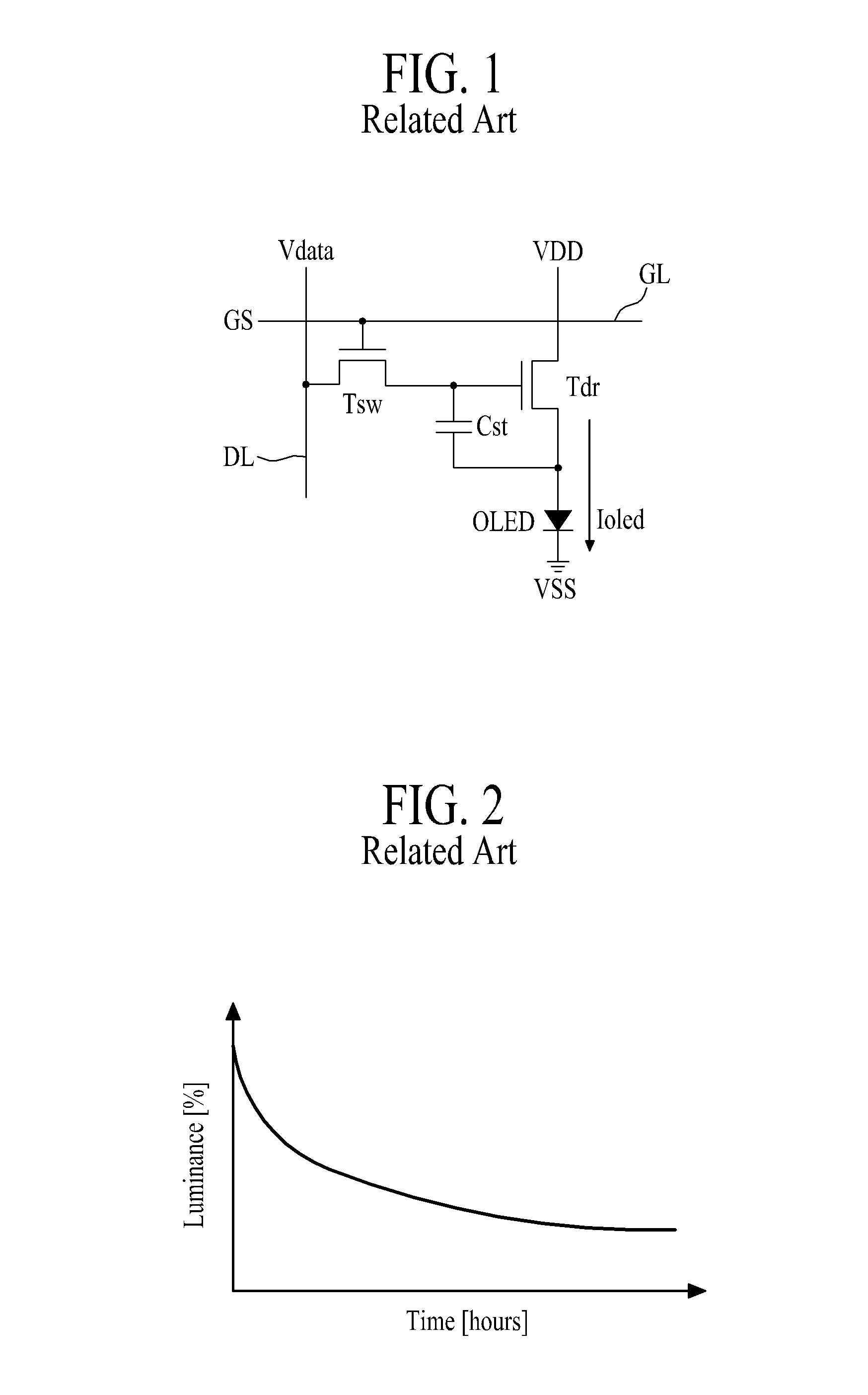
As shown in FIG. 2, the organic light emitting diode (OLED) may degrade as driving time increases, which gradually deteriorates the luminance characteristics.
Thus, the organic light emitting display device according to the related art may have problems of lowered luminance and luminance deviation due to the degradation of the organic light emitting diode (OLED).

Method used


Image

  • Organic light emitting display device and method for driving thereof
  • Organic light emitting display device and method for driving thereof
  • Organic light emitting display device and method for driving thereof

Examples


first embodiment

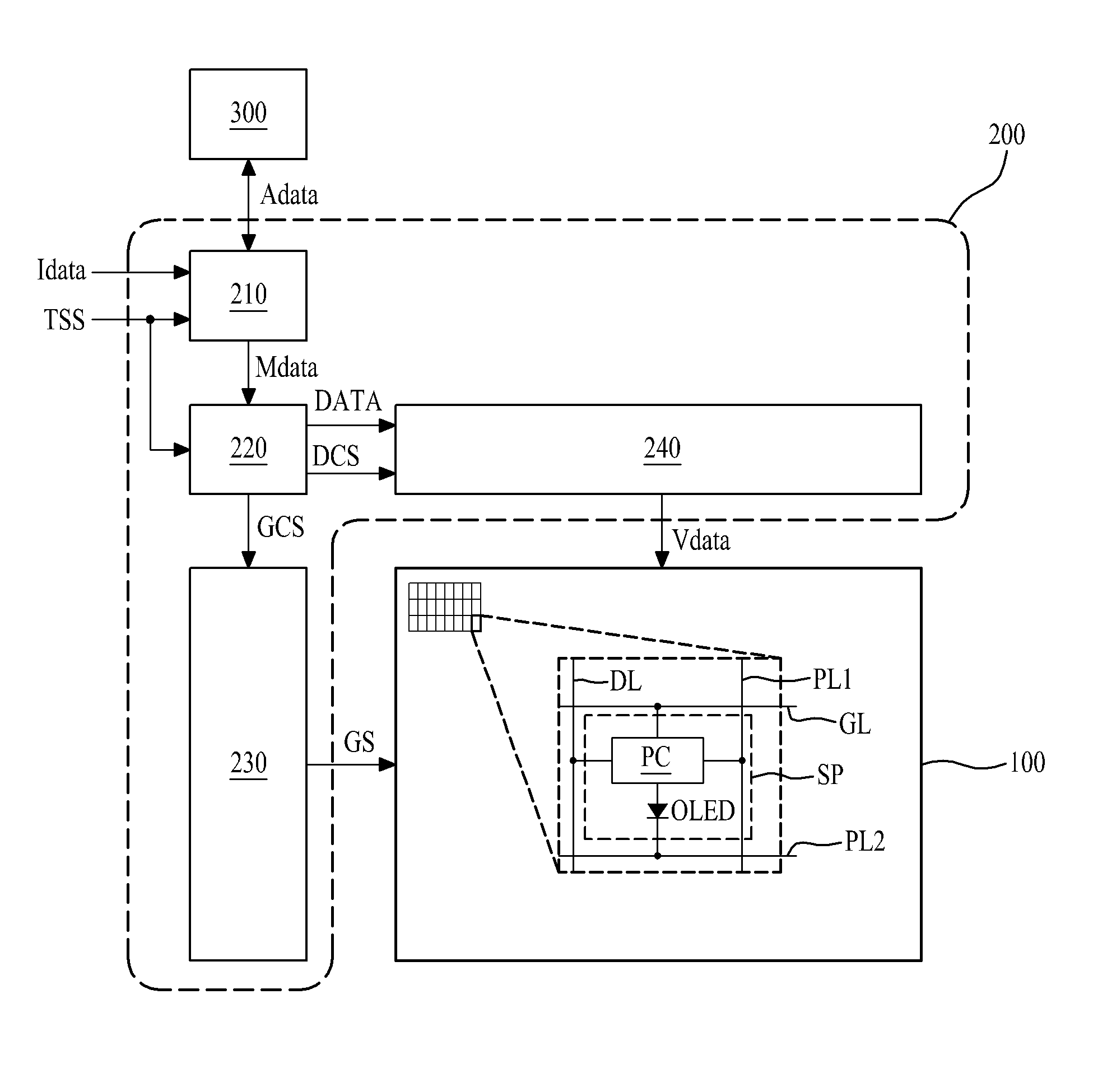
[0057]With reference to FIGS. 4 and 5, the degradation compensator 210 may include a degradation compensation gain value calculator 211, a data modulator 213, and a data accumulator 215.

[0058]The degradation compensation gain value calculator 211 may calculate the degradation compensation gain value (DCG) of each sub-pixel (SP) on the basis of accumulated data of the respective sub-pixels (SP) stored in the memory 300. For example, the degradation compensation gain value calculator 211 calculates the degradation compensation gain value (DCG) for increasing a luminance of each sub-pixel (SP) to a preset initial luminance (or target luminance). In one example, the degradation compensation gain value calculator 211 compares the accumulated data of the corresponding sub-pixel (SP) with compensation point accumulated data (Ref1, Ref2, Ref3). Based on the comparison result, if the accumulated data of the corresponding sub-pixel (SP) is the same as or larger than the compensation point ac...

second embodiment

[0070]FIG. 6 is a block diagram illustrating the degradation compensator, shown in FIG. 3, according to a

[0071]With reference to FIG. 6, the degradation compensator 210 according to the second embodiment may include a degradation compensation gain value calculator 211, a data modulator 213, a degradation weight reflector 214, and a data accumulator 215. Except for the degradation weight reflector 214, the degradation compensator 210 according to the second embodiment may be identical or similar in structure to the degradation compensator of FIGS. 4 and 5 (e.g., according to the first embodiment), and a detailed explanation for the same or similar parts is therefore omitted.

[0072]The degradation weight reflector 214 may calculate a degradation weight by analyzing a grayscale value of modulated data (Mdata) of each sub-pixel (SP) outputted from the data modulator 213, reflect the calculated degradation weight in the modulated data (Mdata) of the corresponding sub-pixel (SP) so as to c...

third embodiment

[0079]FIG. 9 is a block diagram illustrating the degradation compensator, shown in FIG. 3, according to a FIG. 10 is a graph illustrating luminance changes in accordance with the driving time of sub-pixel (SP) in the organic light emitting display device of the embodiment.

[0080]With reference to FIGS. 9 and 10, the degradation compensator 210 according to the third embodiment may include a degradation compensation gain value calculator 3211, a data modulator 3213, and a data accumulator 3215.

[0081]The degradation compensation gain value calculator 3211 may calculate the degradation compensation gain value (DCG) of each sub-pixel (SP) on the basis of accumulated data of the respective sub-pixels (SP) stored in the memory 300. In this case, the degradation compensation gain value calculator 3211 may calculate the degradation compensation gain value (DCG) for decreasing a luminance of each sub-pixel (SP) to a luminance of the sub-pixel (SP) having the organic light emitting diode (OLE...


PUM


Abstract

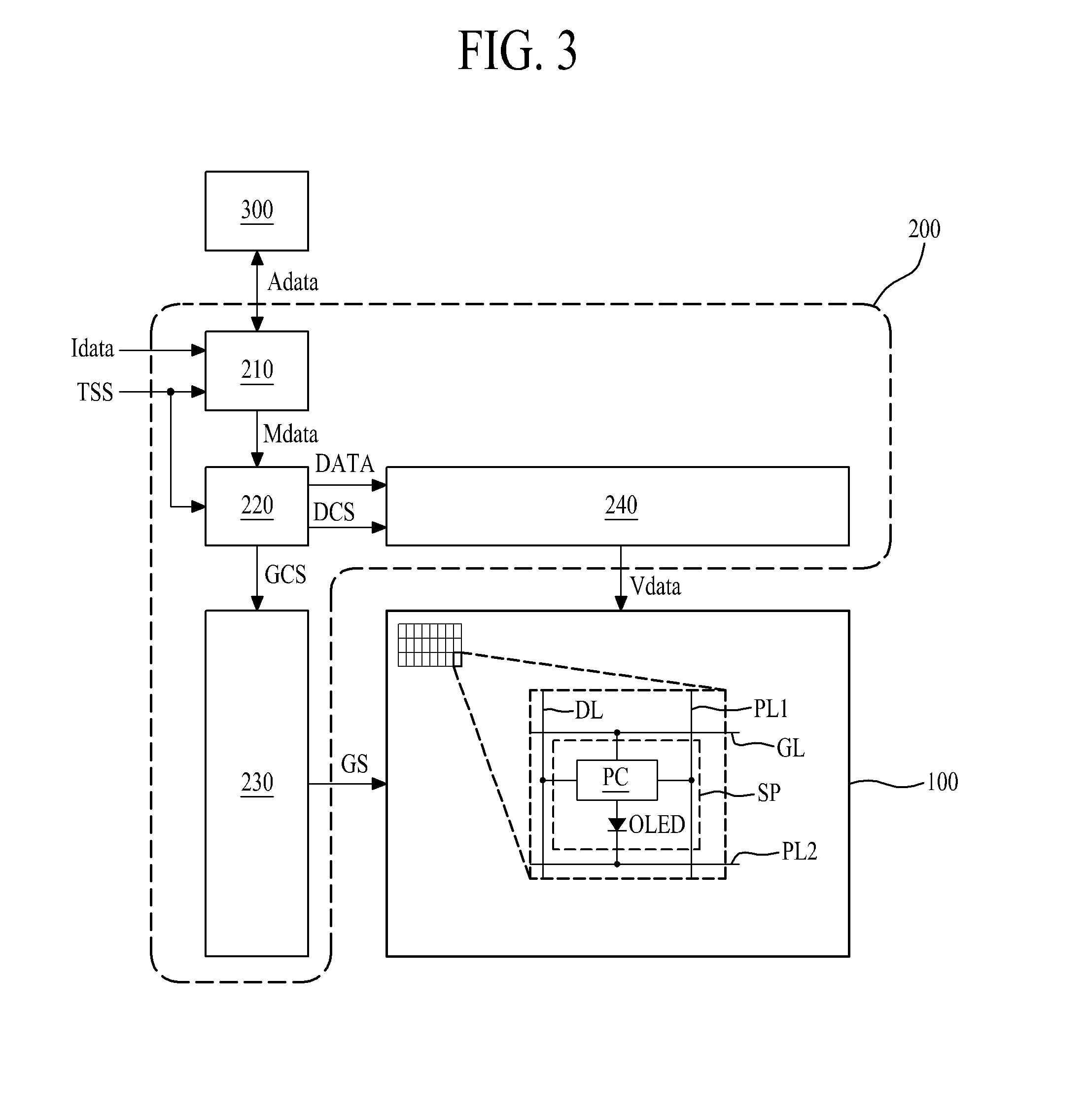
An organic light emitting display device includes a display panel having a plurality of sub-pixels; a memory configured to accumulate and store data displayed by each sub-pixel; and a panel driver configured to: calculate a degradation compensation gain value for increasing or decreasing a luminance of each sub-pixel based on accumulated data of each sub-pixel stored in the memory, generate modulated data of each sub-pixel by modulating input data to each sub-pixel according to the calculated degradation compensation gain value, convert the modulated data into a data voltage, and accumulate the modulated data from the accumulated data of the corresponding sub-pixel and then store the data in the memory.

Description

CROSS REFERENCE TO RELATED APPLICATIONS[0001]This application claims the benefit of priority of Korean Patent Application No. 10-2012-0147930 filed on Dec. 17, 2012, which is hereby incorporated by reference as if fully set forth herein.BACKGROUND[0002]1. Field of the Disclosure[0003]Embodiments relate to an organic light emitting display device and a method for driving the same, for example, to an organic light emitting display device which enables compensating the degradation of an organic light emitting diode, and a method for driving the same.[0004]2. Discussion of the Related Art[0005]According to recent developments in multimedia, there is increasing demand for flat panel displays. To satisfy this increasing demand, various flat panel displays such as liquid crystal display devices, plasma display panels, field emission display devices and organic light emitting display devices are used in practice. Among the various flat panel displays, the organic light emitting display devi...

Claims


Application Information

Patent Timeline
IPC IPC(8): G09G3/32
CPCG09G3/3233G09G3/3275G09G2300/0842G09G2320/043G09G2320/048G09G2360/16G09G3/30G09G3/3208
Inventor KIM, HYUNG RAEBYUN, SEUNG CHANYI, JUNG YOONCHOI, KYOUNG SIKPARK, DAE HYEONJEONG, UI TAEKBYEON, BOEON
Owner LG DISPLAY CO LTD
Learn More