Distortion measurement for limiting jitter in pam transmitters

a technology of distortion measurement and jitter limitation, which is applied in the field of high-speed communication, can solve problems such as reducing the noise immunity of the receiver, allowing deviations from the specified values, and the clock of the receiver sampling at incorrect times

Active Publication Date: 2014-06-19
INTEL CORP
View PDF2 Cites 16 Cited by
  • Summary
  • Abstract
  • Description
  • Claims
  • Application Information

AI Technical Summary

Problems solved by technology

The voltage deviations create noise that adds up to other noise sources and reduces the noise immunity of the receiver.
The timing deviations may also be considered as additional noise, and might also cause the receiver clock to sample at incorrect times. Thus, communication standards that specify voltages and frequencies typically limit the allowed deviations from the specified values.
High frequency jitter is created either from PLL phase noise or from other causes; it is assumed to be impossible to track, and thus must be limited to prevent sampling errors in the receiver.
At very high speeds, the communication medium is band limited and inter-symbol interference (ISI) becomes significant.
ISI causes both voltages and transition times to change; thus a signal observed through an ISI medium will have increased jitter, which cannot be tracked by the receiver.
If not handled, ISI-induced jitter can become a performance bottleneck; indeed, jitter measurement methods for optical links require using test signals that reveal the maximum effect of ISI, such as PRBS31 (31-bit Pseudo-random bit sequence).
For the 40 GBASE-CR4 and 100 GBASE-CR10 cases, such measurements are problematic, since the lossy PCB can distort the test pattern and increase the measured “noise” (Δv2 and Δv5) although it is actually a linear effect that is mitigated by equalization.
There are four major problems with these specification methods.
First, both jitter and noise measurement methods are specific to PAM2 modulation, and cannot be easily translated to higher-order PAM schemes, such as PAM4 (4-level) which is used in 100 GBASE-KP4.
Second, since both jitter and noise are transmitter effects that contribute to noise seen by the receiver, it would be better to limit their combined effect, rather than each one separately.
Combining the specifications is difficult since jitter is measured and defined in time unit, while noise is measured and defined in voltage units.
Third, the measurement contains many steps, some of which require non-trivial calculations that are typically done by specialized test equipment.
Fourth, It is difficult to justify the limits defined for each of the effects with standard system engineering methods such as noise budgeting.
The limits specified represent some agreement between engineers that building such transmitters are feasible, and that such transmitters should be “good enough” for operation in the specified standard (which also define channels and receivers), but there is no proof or rigorous analysis.

Method used


Image

  • Distortion measurement for limiting jitter in pam transmitters
  • Distortion measurement for limiting jitter in pam transmitters
  • Distortion measurement for limiting jitter in pam transmitters

Examples


Embodiment Construction

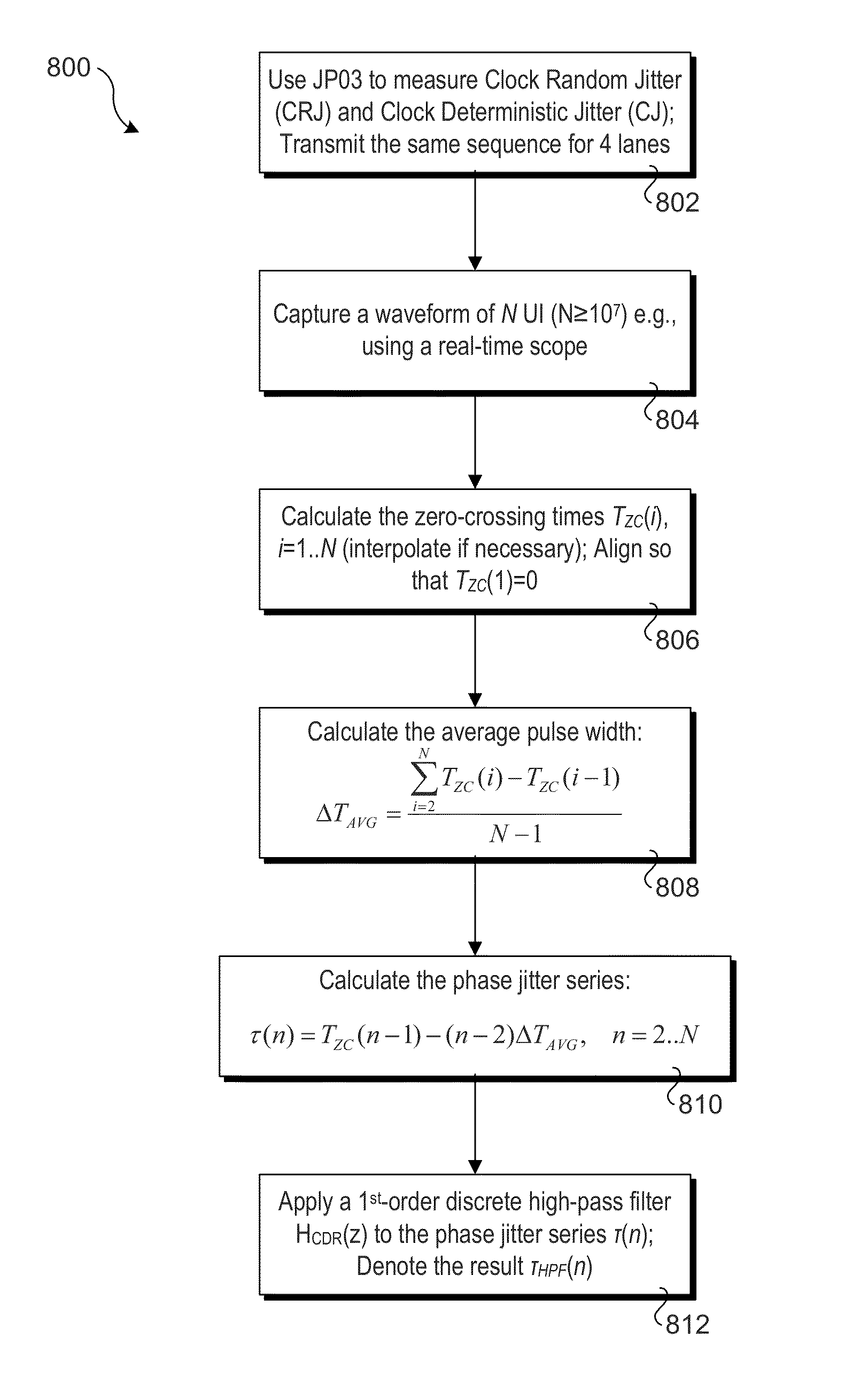
[0030]Embodiments of methods and apparatus for measuring jitter in Pulse Amplitude Modulated transmitters are described herein. In the following description, numerous specific details are set forth to provide a thorough understanding of embodiments of the invention. One skilled in the relevant art will recognize, however, that the invention can be practiced without one or more of the specific details, or with other methods, components, materials, etc. In other instances, well-known structures, materials, or operations are not shown or described in detail to avoid obscuring aspects of the invention.

[0031]Reference throughout this specification to “one embodiment” or “an embodiment” means that a particular feature, structure, or characteristic described in connection with the embodiment is included in at least one embodiment of the present invention. Thus, the appearances of the phrases “in one embodiment” or “in an embodiment” in various places throughout this specification are not n...


PUM


Abstract

Methods and test equipment for measuring jitter in a Pulse Amplitude Modulated (PAM) transmitter. Under one procedure, a first two-level PAM signal test pattern is used to measure clock-related jitter separated into random and deterministic components, while a second two-level PAM signal test pattern is used to measure oven-odd jitter (EOJ). Under another procedure, A four-level PAM signal test pattern is used to measure jitter-induced noise using distortion analysis. Test equipment are also disclosed for implementing various aspects of the test methods.

Description

FIELD OF THE INVENTION[0001]The field of invention relates generally to high-speed communications and, more specifically but not exclusively relates to techniques for measuring jitter in Pulse Amplitude Modulated transmitter.BACKGROUND INFORMATION[0002]In high-speed signaling communication standards, the transmitted data is converted by a physical medium-dependent (PMD) device to a physical voltage signal. Ideally, the voltage signal should have one of M several possible voltage levels (e.g., M=2 for the PAM2 (Pulse Amplitude Modulated 2-level) signaling scheme, which maps “0” bits to one voltage level and “1” bits to another voltage level). The transitions between these levels should occur only at specific times (integer multiples of a “unit interval” or UI) that correspond to a perfect clock. A clock with the same frequency is used in a receiver in order to sample the received signal and reconstruct the transmitted data.[0003]In practice, the voltage levels generated by transmitte...

Claims


Application Information

Patent Timeline
Patent Type & Authority Applications(United States)
IPC IPC(8): H04L1/24
CPCH04L1/248H04B17/104G01R29/027G01R31/31709H04L1/205H04L1/24H04L27/04
Inventor RAN, ADEE, O.
Owner INTEL CORP
Why Eureka
Try Eureka