Method for bonding semiconductor substrates and devices obtained thereof

a technology of semiconductor substrates and substrates, which is applied in the direction of semiconductor devices, semiconductor/solid-state device details, electrical equipment, etc., can solve the problems of compromising reliability and hence the yield of 3d devices, high manufacturing cost, and cu has a tendency to develop oxides and other contaminants, so as to improve the roughness of metal surfaces, reduce the time duration of scrubbing, and reduce the effect of pressur

Active Publication Date: 2014-06-19
INTERUNIVERSITAIR MICRO ELECTRONICS CENT (IMEC VZW) +1
View PDF1 Cites 2 Cited by
  • Summary
  • Abstract
  • Description
  • Claims
  • Application Information

AI Technical Summary

Benefits of technology

[0013]An advantage of the mechanical scrubbing step over other methods for the removal of oxides and contaminants from the metal contact structures, is that it is compatible with current high volume semiconductor manufacturing processes. Furthermore, the mechanical scrubbing step can be performed at a location which is independent from the manufacturing of the semiconductor substrates. This is a major advantage, especially in the case whereby semiconductor substrates from different manufacturer are bonded in a third party location, such a packaging house.
[0014]In certain embodiments, a low pressure force can be applied during the mechanical scrubbing step. By applying a low pressure force during mechanical scrubbing the time duration for which scrubbing is performed can be reduced. This is highly beneficial in the case wherein a substantial layer of oxide and / or contaminants has been formed on the metal surfaces. The pressure applied during this step is preferably between 3.5 MPa and 14 MPa.
[0015]Applying a pressure during the mechanical scrubbing step has the additional advantage of improving the roughness of the metal surfaces. As a result, a planarization of the metal surfaces is achieved. The planarization of metal surfaces has been found to contribute significantly in lowering the temperature and pressure applied during TC-bonding and improving reliability. Therefore it is desirable to provide the contact structures with substantially planar metal surfaces.
[0016]It is further desirable to combine the mechanical scrubbing method with conventional techniques for further improving the planarization of the surfaces of the metal contact structures, for example Chemical Mechanical Polishing (CMP), or fly cutting process using a single-crystalline diamond turning tool. These techniques are traditionally performed prior to the TC-bonding for the same purpose; however, their effectiveness is limited at planarizing surfaces at a micro / nano level and for removing substantially thicker oxide and / or contaminant layers. In the planarization of metal surfaces the use of fly cutting is preferred over the CMP, due to its speed of operation and less abrasive nature.
[0017]It has been found, that the combination of fly-cutting and mechanical scrubbing can significantly further reduce the temperature, pressure and time required during bonding. Therefore, by introducing the step of mechanical scrubbing TC-bonding can be performed at the following conditions: at a temperature between 150° C. and 300° C., and more preferably at around 220° C., at a pressure between 10 MPa and 300 MPa, and more preferably at 20 MPa, and for a duration between around 1 second and 5 minutes, and more preferably 45 seconds.

Problems solved by technology

However, reliability and the high cost of manufacturing remain the main issues that prevent 3D technology to be adopted in volume production.
These issues are mainly associated with the bonding of semiconductor substrates and more specifically with the material selection and bonding methods used therein.
On the other hand, Cu has a tendency to develop oxides and other contaminants during manufacturing.
As a result of the high temperature and high pressure applied during TC-bonding, stress related failures might occur in the bonded semiconductor substrates, thereby compromising reliability and hence yield of the 3D device manufactured.
Moreover, the conditions for performing TC-bonding, limit the applications that could benefit from Cu—Cu bonding.
As an example, a memory chip containing DRAM or SRAM cells will not be able to withstand the temperature and forces applied during thermo-compression bonding.
The proposed process flows are carried out in a controlled process environment and requires complex processing steps, for example the chemical cleaning step, that are incompatible with current high volume semiconductor manufacturing processes.

Method used


Image

  • Method for bonding semiconductor substrates and devices obtained thereof
  • Method for bonding semiconductor substrates and devices obtained thereof
  • Method for bonding semiconductor substrates and devices obtained thereof

Examples


Embodiment Construction

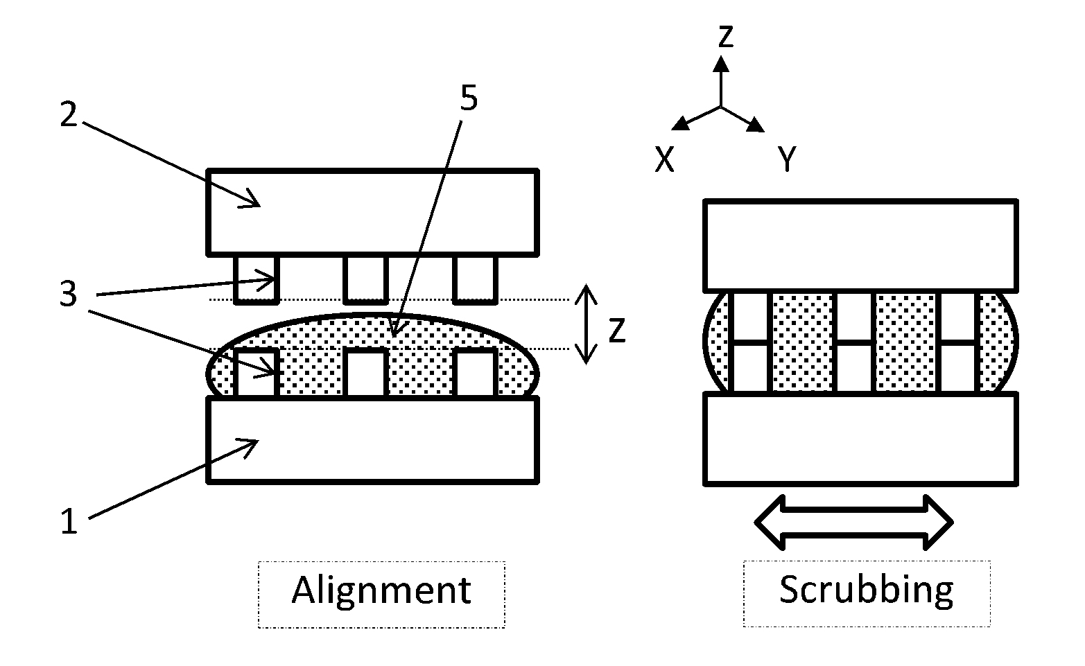
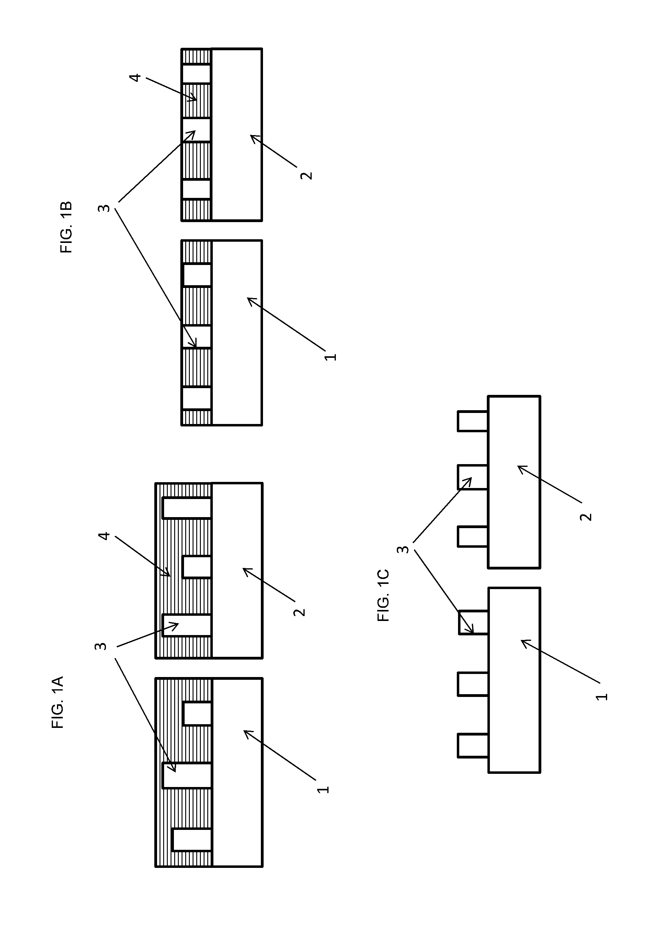
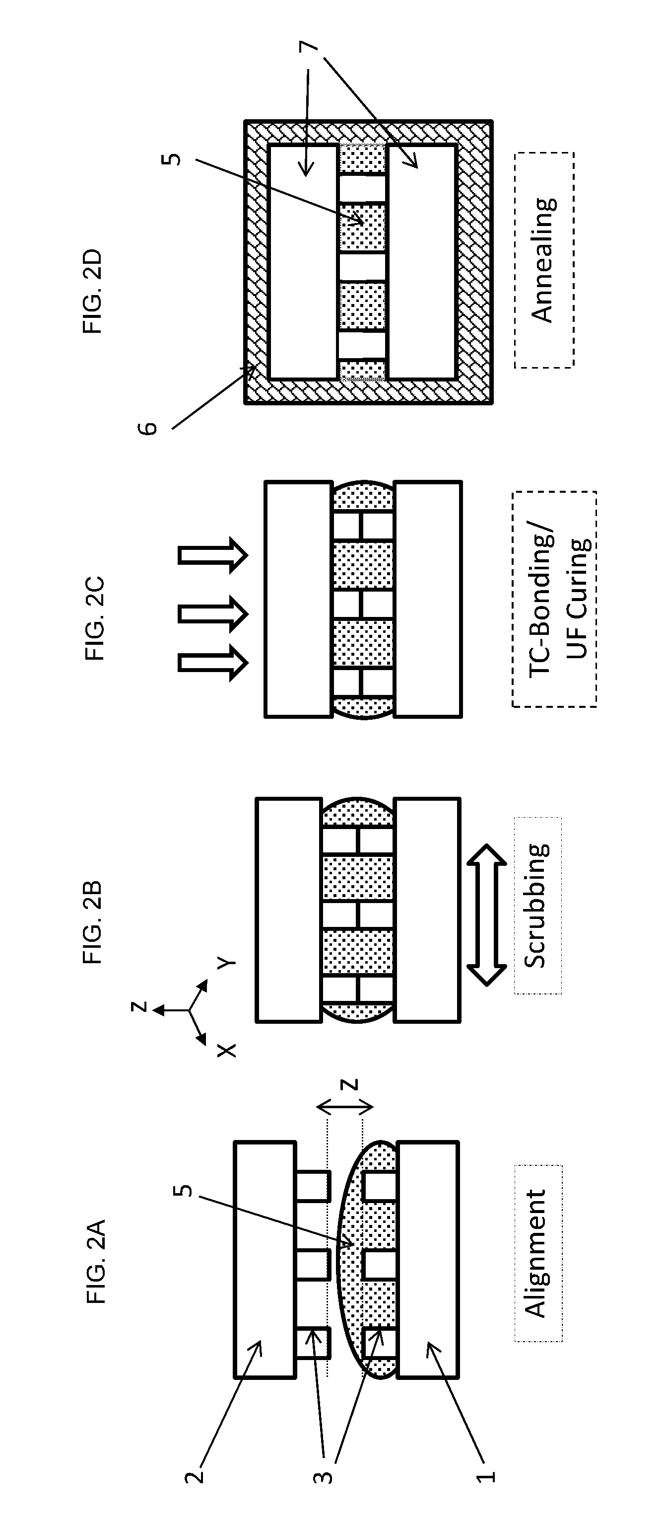
[0032]The present disclosure will be described with respect to particular embodiments and with reference to certain drawings but the disclosure is not limited thereto but only by the claims. The drawings described are only schematic and are non-limiting. In the drawings, the size of some of the elements may be exaggerated and not drawn on scale for illustrative purposes.

[0033]Moreover, the term top and the like in the description and the claims are used for descriptive purposes and not necessarily for describing relative positions. It is to be understood that the terms so used are interchangeable under appropriate circumstances and that the preferred embodiments described herein are capable of operation in other orientations than described or illustrated herein.

[0034]Reference throughout this specification to “one embodiment” or “an embodiment” means that a particular feature, structure or characteristic described in connection with the embodiment is included in at least one embodim...


PUM

PropertyMeasurementUnit
pressureaaaaaaaaaa
time durationaaaaaaaaaa
temperatureaaaaaaaaaa

Abstract

A method is provided for bonding a first semiconductor substrate to a second semiconductor substrate using low temperature thermo-compression. The bonding method comprises the step of in-situ mechanically scrubbing the metal contact structure surfaces prior to thermo-compression bonding step, thereby planarizing the removing the oxides and/or contaminants from the metal contact structure surfaces. The thermo-compression bonding step is followed by a thermal annealing step for creating interface diffusion between the metal contact structure of the first and second semiconductor substrates

Description

INCORPORATION BY REFERENCE OF RELATED APPLICATION[0001]Any and all priority claims identified in the Application Data Sheet, or any correction thereto, are hereby incorporated by reference under 37 CFR 1.57. This application claims the benefit of European Patent Application No. 12197425.7, filed Dec. 17, 2012, the disclosure of which is hereby expressly incorporated by reference in its entirety and is hereby expressly made a portion of this application.FIELD OF THE INVENTION[0002]Methods for three-dimensional stacking of semiconductor substrates and more in particular to a method of bonding semiconductor substrates using thermo-compression are provided.BACKGROUND[0003]Three-Dimensional (3D) stacking of semiconductor substrates is a promising technology for manufacturing devices with improved performance and power consumption while maintaining a low form factor. Over the past few years, numerous technological advances in the field of 3D technology have been reported. However, reliabi...

Claims


Application Information

Patent Timeline
Patent Type & Authority Applications(United States)
IPC IPC(8): H01L23/00
CPCH01L24/11H01L24/81H01L24/13H01L24/16H01L2224/05568H01L2224/05647H01L2224/05644H01L2224/05624H01L2224/11009H01L2224/13023H01L2224/13009H01L2224/11845H01L2224/13147H01L2224/16146H01L2224/16148H01L2224/73204H01L2224/73104H01L2224/8183H01L2224/81986H01L2224/81948H01L2224/81002H01L2224/81012H01L2224/8121H01L2224/81047H01L2224/81203H01L2224/81193H01L2224/81191H01L2224/83862H01L2224/83047H01L2224/83191H01L2224/83203H01L2224/9221H01L2924/00014H01L2924/00012H01L2224/13124H01L2224/13144H01L2224/0401H01L2224/81H01L2224/83H01L2224/05552H01L24/83
Inventor HU, YU-HSIANGLIU, CHUNG-SHI
Owner INTERUNIVERSITAIR MICRO ELECTRONICS CENT (IMEC VZW)
Why Eureka
Try Eureka