Nitride semiconductor light emitting device and method of manufacturing the same

a technology of semiconductor light emitting device and nitride, which is applied in the manufacturing of semiconductor/solid-state devices, semiconductor devices, and semiconductor devices, etc., can solve the problems of rapid deterioration in bonding reliability, improve light scattering capability, and enhance long-term reliability.

Inactive Publication Date: 2014-07-03
ILJIN LED
View PDF16 Cites 15 Cited by
  • Summary
  • Abstract
  • Description
  • Claims
  • Application Information

AI Technical Summary

Benefits of technology

[0012]In the light emitting device according to the present invention, the current blocking pattern is formed on the p-type nitride layer, the transparent conductive pattern having a contact hole is formed on the p-type nitride layer and the current blocking pattern to improve light scattering...

Problems solved by technology

In this case, since the transparent conductive pattern and the p-electrode pad are formed of metallic mater...

Method used


Image

  • Nitride semiconductor light emitting device and method of manufacturing the same
  • Nitride semiconductor light emitting device and method of manufacturing the same
  • Nitride semiconductor light emitting device and method of manufacturing the same

Examples


Embodiment Construction

[0018]Exemplary embodiments of the present invention will now be described in detail with reference to the accompanying drawings.

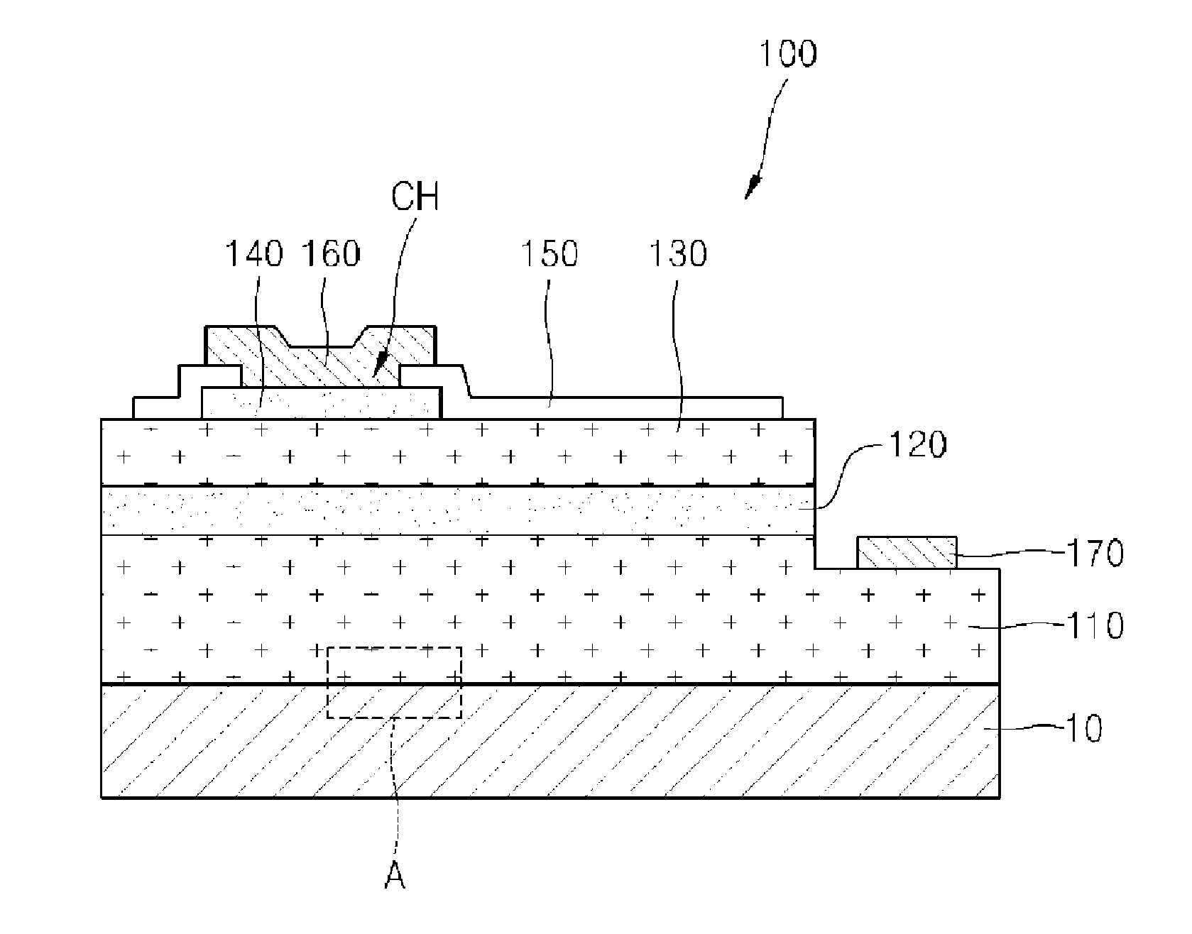
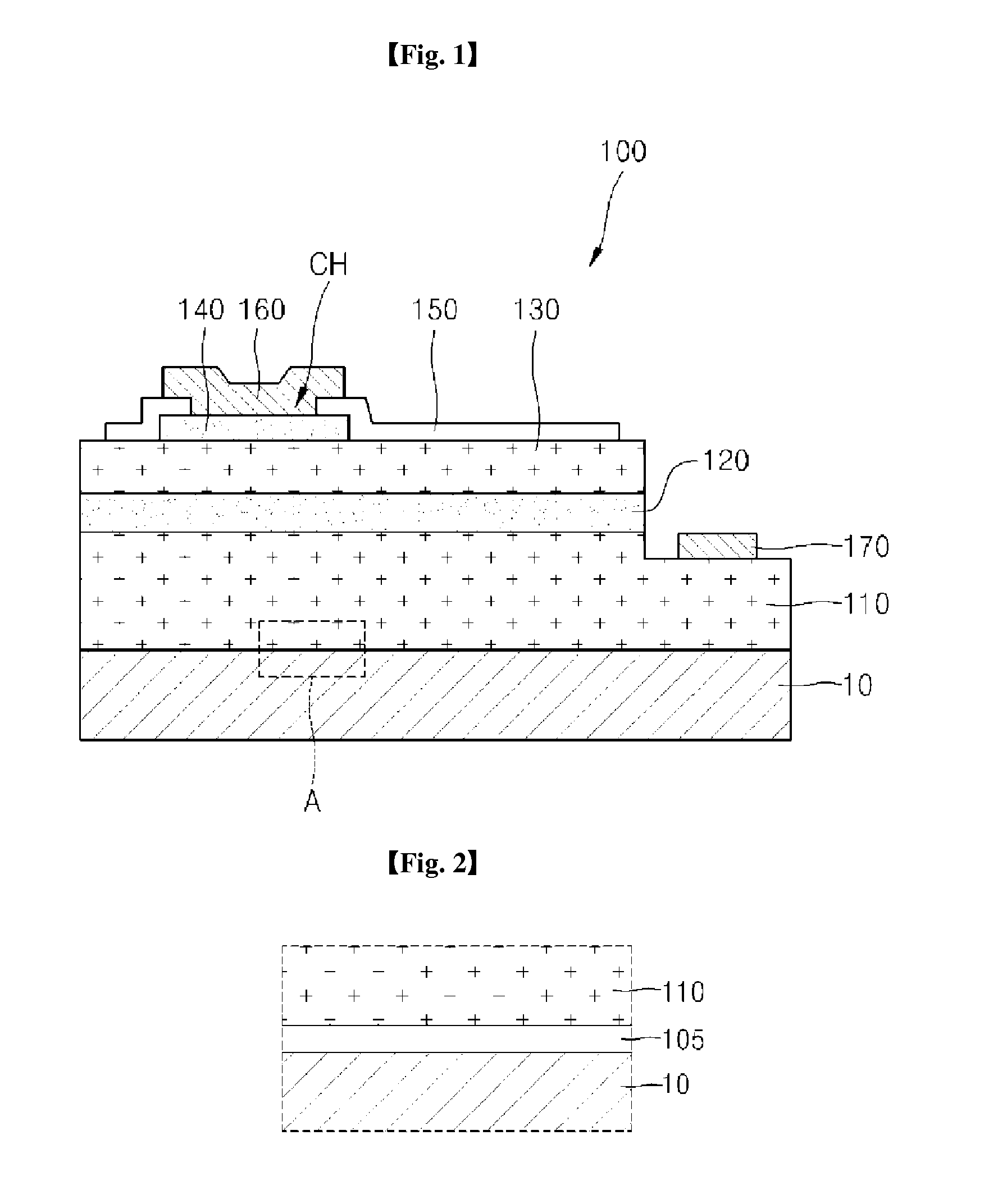
[0019]FIG. 1 is a sectional view of a nitride semiconductor light emitting device according to one embodiment of the present invention and FIG. 2 is a partially enlarged view of part A in FIG. 1.

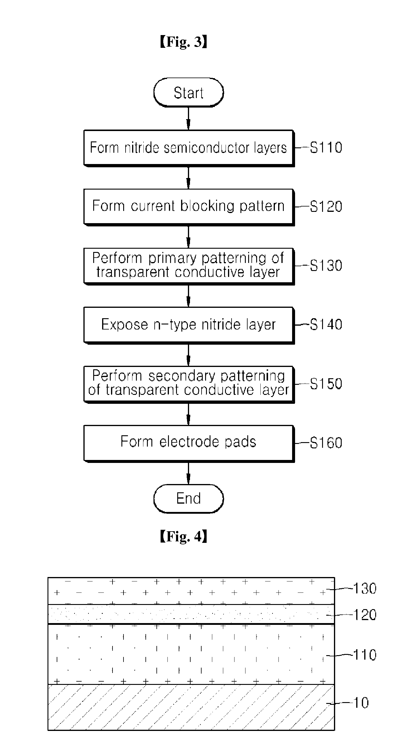
[0020]Referring to FIGS. 1 and 2, a nitride semiconductor light emitting device 100 according to one embodiment of the invention includes an n-type nitride layer 110, an active layer 120, a p-type nitride layer 130, a current blocking pattern 140, a transparent conductive pattern 150, a p-electrode pad 160, and an n-electrode pad 170. The nitride semiconductor light emitting device 100 may further include a buffer layer 105.

[0021]The n-type nitride layer 110 is formed on a substrate 10 or on the buffer layer 105. The n-type nitride layer 110 may have a stack structure in which first silicon (Si)-doped AlGaN layers (not shown) and second undoped GaN layers are alter...


PUM


Abstract

A nitride semiconductor light emitting device and a method of manufacturing the same are disclosed. The nitride semiconductor light emitting device includes an n-type nitride layer; an active layer formed on the n-type nitride layer; a p-type nitride layer formed on the active layer; a current blocking pattern formed on the p-type nitride layer; a transparent conductive pattern formed to cover upper sides of the p-type nitride layer and the current blocking pattern, and having a contact hole through which a portion of the current blocking pattern is exposed; and a p-electrode pad formed on the current blocking pattern and the transparent conductive pattern, and directly connected to the current blocking pattern. The nitride semiconductor light emitting device can improve long term durability by securing excellent light scattering properties while enhancing adhesion of a p-electrode pad.

Description

CROSS-REFERENCE TO RELATED APPLICATION[0001]This application claims priority to Korean Patent Application No. 10-2012-0156369 filed on Dec. 28, 2013, and all the benefits accruing therefrom under 35 U.S.C. §119, the contents of which is incorporated by reference in its entirety.BACKGROUND[0002]1. Technical Field[0003]The present invention relates to a semiconductor light emitting device and a method of manufacturing the same. More particularly, the present invention relates to a nitride semiconductor light emitting device which has excellent light scattering capabilities and adhesion, and a method of manufacturing the same.[0004]2. Description of the Related Art[0005]In recent years, gallium nitride (GaN)-based nitride semiconductor light emitting devices have been mainly studied as nitride semiconductor light emitting devices. Such a GaN-based nitride semiconductor light emitting device is used in various applications, including blue and green light emitting diodes (LEDs), high spe...

Claims


Application Information

Patent Timeline
IPC IPC(8): H01L33/38H01L33/44H01L33/42
CPCH01L33/38H01L33/44H01L33/42H01L33/145H01L33/36
Inventor KIM, SEUNG-YONGHONG, JEONG-WOO
Owner ILJIN LED
Why Eureka
Try Eureka