Plane light source device and preparation method thereof

A flat light source and device technology, applied in the manufacture of semiconductor/solid-state devices, electric solid-state devices, semiconductor devices, etc., can solve the problems of low luminous brightness and have not been widely commercialized, and achieve the effect of improving the brightness of the light source

Inactive Publication Date: 2010-08-04
IRICO
View PDF2 Cites 4 Cited by
  • Summary
  • Abstract
  • Description
  • Claims
  • Application Information

AI Technical Summary

Problems solved by technology

The planar light source of organic light-emitting diodes (OLEDs), which has attracted widespread attention, has many advantages, such as: less shadows, low energy consumption, low operating voltage, safe use and maintenance, uniform light emission, no flicker, etc., but because the material emits light Low brightness and not widely used commercially

Method used


Image

  • Plane light source device and preparation method thereof
  • Plane light source device and preparation method thereof

Examples


Embodiment 1

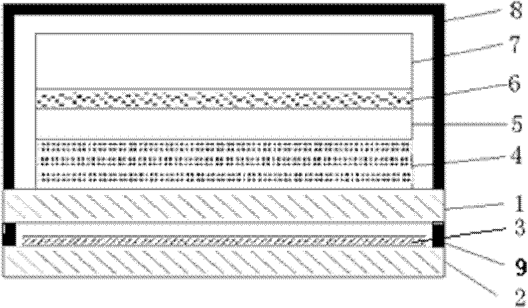
[0023] Example 1, please refer to figure 1 :

[0024] Step 1: Weigh 5g of ethyl cellulose and 45g of terpineol, put them in a clean beaker, stir at a constant temperature of 70°C-80°C for 2-3h, prepare a carrier, and transfer it to a mortar;

[0025] Step 2: Weigh 50g of CCFL phosphor, the particle size of which is 6.8μm, 0.3g of BYK171 dispersant, 0.4g of hydroxydimethylsiloxane as defoaming agent, and 1g of silicon dioxide, of which , the particle size of silicon dioxide is less than 1 μm, put it into a mortar filled with the above-mentioned carrier and grind together for half an hour to make a phosphor powder slurry for later use;

[0026] The third step: the lower glass substrate 2, which is ultra-clear glass used in this embodiment, is cleaned with detergent and dried, and then printed on it with a thickness of 10 μm prepared in the second step by screen printing. phosphor paste, thereby forming a phosphor layer 3;

[0027] The 4th step: A) will have the upper glass su...

Embodiment 2

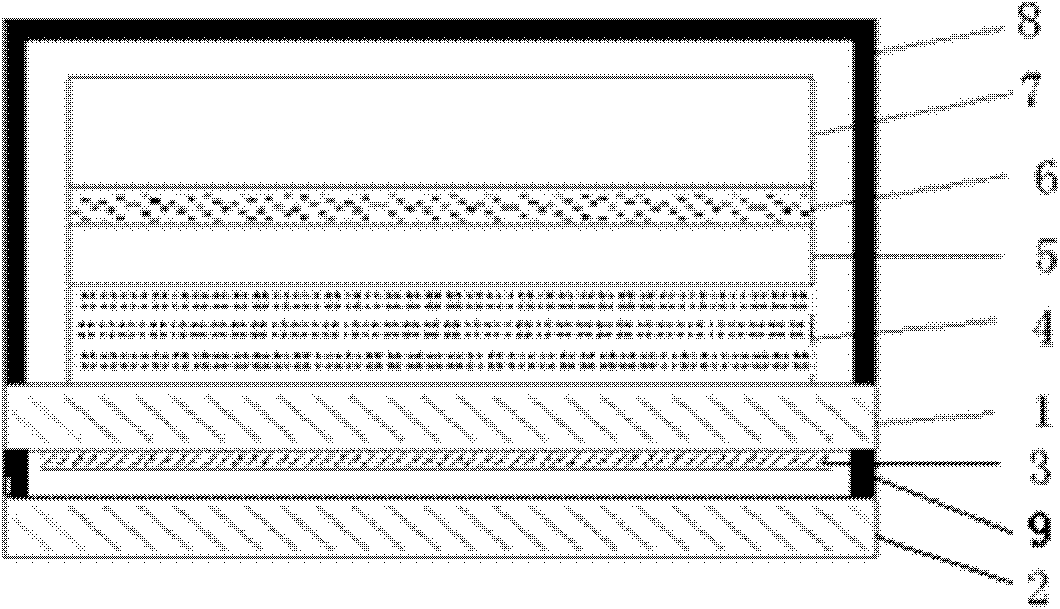
[0033] Example 2, please refer to figure 2 Shown:

[0034] The difference between this embodiment and Embodiment 1 is that the phosphor layer 3 is prepared on the lower surface of the upper glass substrate 1, that is, the upper glass substrate 1 with indium tin oxide (ITO) is cleaned and dried on the upper glass substrate. 1 Print a layer of phosphor paste on the side without the ITO conductive layer by screen printing, thereby forming a phosphor layer 3 with a thickness of 10 μm. The other production processes are the same, and will not be repeated here.

[0035] Table 1 is a comparison of relevant data between the light source device of the present invention and the traditional light source device, wherein A1-A3 are traditional light sources, that is, planar dielectric barrier discharge light sources, and B1-B3 are planar light sources of the present invention:

[0036] Table 1

[0037] serial number


PUM

PropertyMeasurementUnit
thicknessaaaaaaaaaa
thicknessaaaaaaaaaa

Abstract

The invention discloses a plane light source device and a preparation method thereof. The preparation method is characterized in that the bonding force of fluorescent powder and glass substrate can be improved and the luminance of the light source can be improved by adding silica particles when fluorescent powder sizing agent is prepared.

Description

【Technical field】 [0001] The invention relates to the field of organic optoelectronics, in particular to a planar light source device and a preparation method thereof. 【Background technique】 [0002] Planar light sources are widely used in various fields, for example, as backlight sources for liquid crystal displays. Planar light sources are usually made from a linear light source such as a cold cathode fluorescent (CCFL) tube together with a planar (two-dimensional) light directing / diffusing layer to scatter light in a plane from which it can be scattered. [0003] A point light source, such as a small lamp or a two-dimensional array of other light sources such as light-emitting diodes, is also considered a planar light source to a certain extent, but the cost is relatively high; a field emission device (FED) that uses an electron beam inside a vacuum tube to excite a fluorescent layer is also considered to be a flat light source. It can be considered as a display device o...

Claims


Application Information

Patent Timeline
Patent Type & Authority Applications(China)
IPC IPC(8): H01L51/56H01L51/50H01L51/52H01L51/54
Inventor 王香
Owner IRICO
Why Eureka
Try Eureka