Imaging device, semiconductor integrated circuit and imaging method

Active Publication Date: 2014-07-03
PANASONIC INTELLECTUAL PROPERTY MANAGEMENT CO LTD
View PDF36 Cites 89 Cited by
  • Summary
  • Abstract
  • Description
  • Claims
  • Application Information

AI Technical Summary

Benefits of technology

[0016]An image capture device according to the present disclosure gets a focus lens displaced in two ranges, of which the displacement ranges are separate from each oth

Problems solved by technology

When an image is captured through a microscope, the object of shooting is a still object, and therefore, the shooter can take a lot of time to shoot such an object.
However,

Method used


Image

  • Imaging device, semiconductor integrated circuit and imaging method
  • Imaging device, semiconductor integrated circuit and imaging method
  • Imaging device, semiconductor integrated circuit and imaging method

Examples


Example

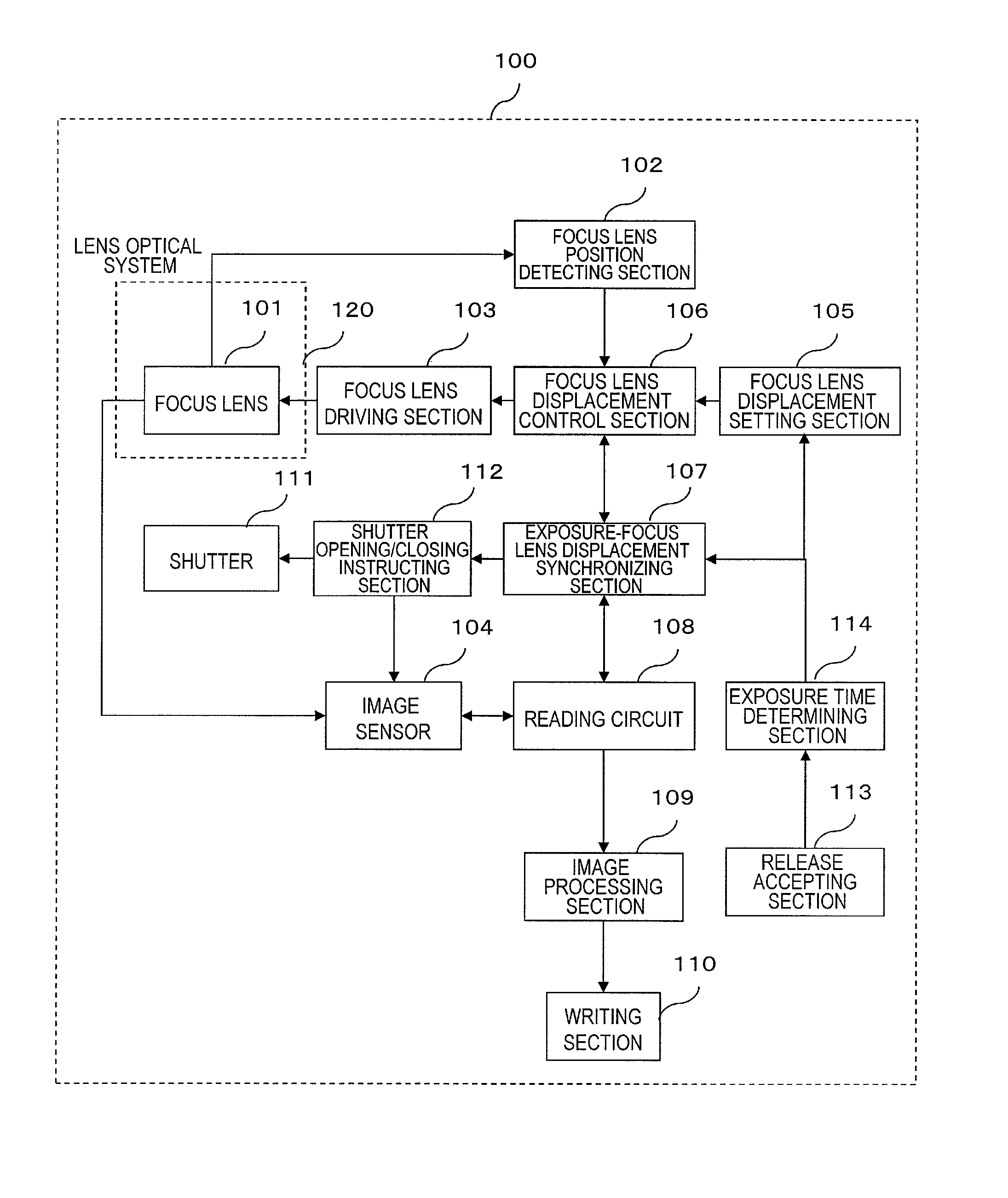
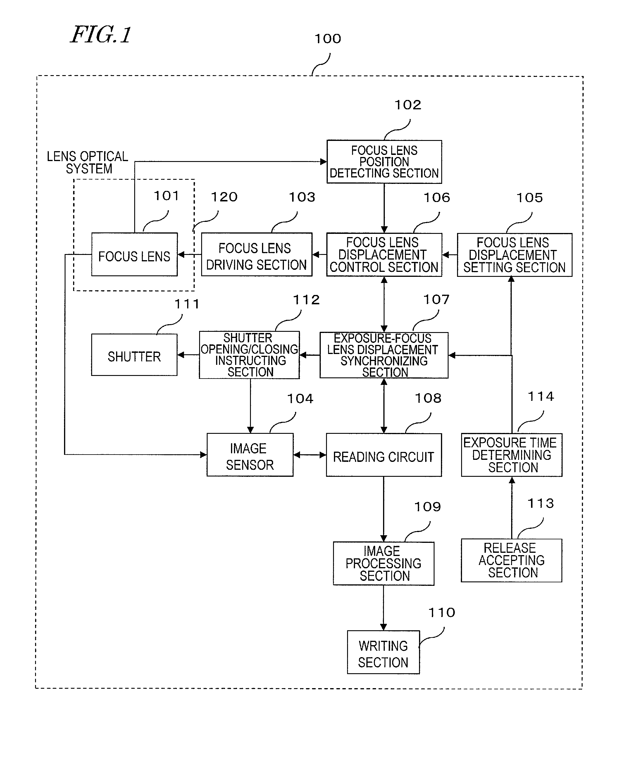
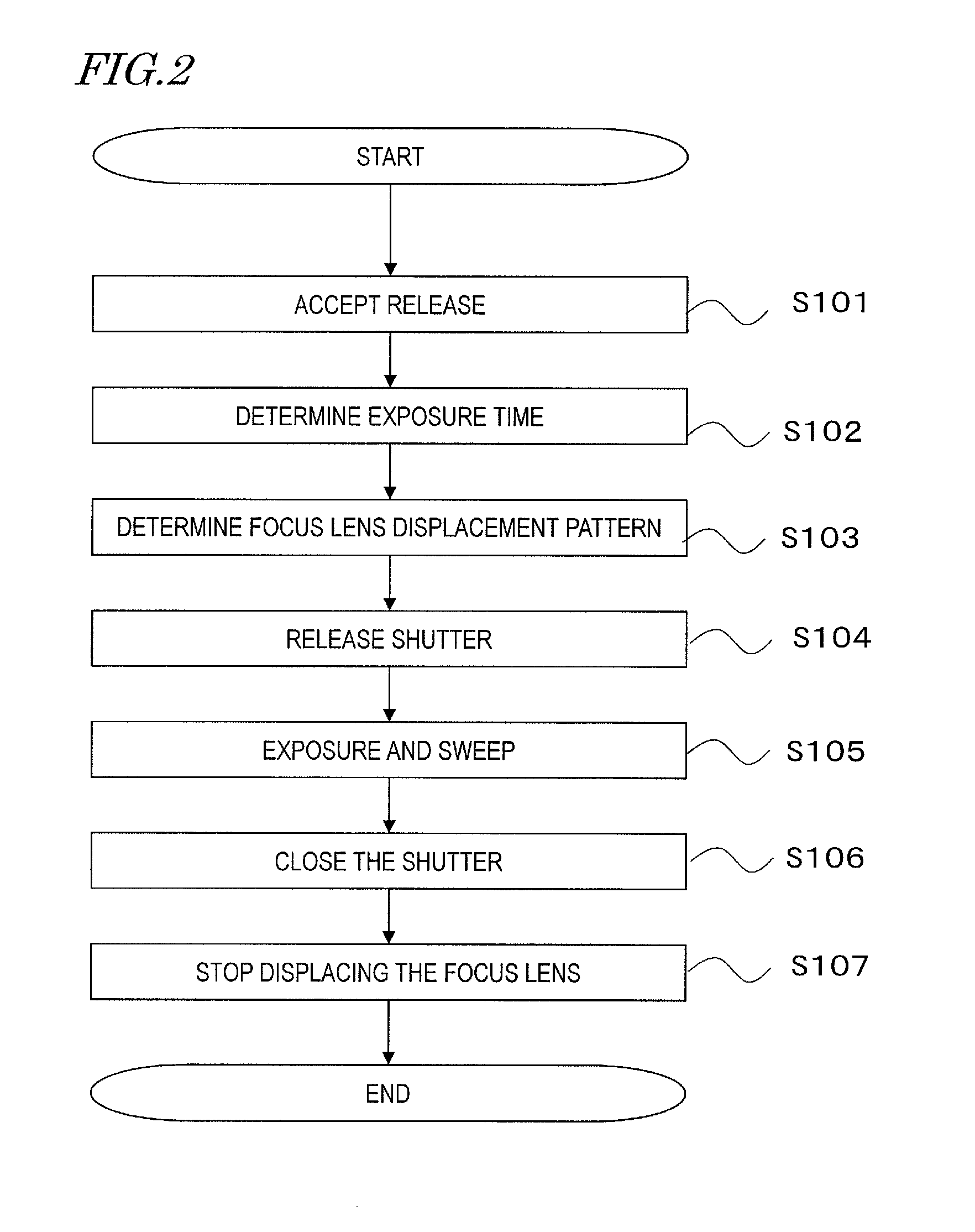
[0093]Hereinafter, a first embodiment of an image capture device, integrated circuit and image capturing method according to the present invention will be described with reference to the accompanying drawings.

[0094]FIG. 1 is a block diagram illustrating a configuration for an image capture device 100 as a first embodiment. The image capture device 100 includes a focus lens driving section 103, an image sensor 104, a focus lens displacement control section 106, an exposure-focus lens displacement synchronizing section 107, and a lens optical system 120.

[0095]The image sensor 104 may be a CCD image sensor in this embodiment, and includes a plurality of photoelectric conversion elements that are arranged two-dimensionally to form an image capturing plane. The image sensor 104 gets the plurality of photoelectric conversion elements exposed to light and reads an electrical signal from the plurality of photoelectric conversion elements, thereby generating an image signal;

[0096]The lens op...

Example

[0133]Hereinafter, a second embodiment of an image capture device, integrated circuit and image capturing method according to the present invention will be described with reference to FIGS. 5 and 6.

[0134]FIG. 5 is a block diagram illustrating a configuration for an image capture device 200 according to this embodiment. In FIG. 5, any component also included in the image capture device 100 of the first embodiment and having substantially the same function as its counterpart is identified by the same reference numeral. This image capture device 200 changes the distance from the focus lens 101 of the lens optical system 120 by moving the image sensor 104, which is different from the image capture device 100.

[0135]For that purpose, this image capture device 200 includes an image sensor position detecting section 202, an image sensor driving section 203, an image sensor displacement setting section 205, an image sensor displacement control section 206, and an exposure-image sensor displa...

Example

Embodiment 3

[0142]The image capture devices of the first and second embodiments use a CCD image sensor as their image sensor. As a CCD image sensor can perform a global shutter operation, by which all pixels can be scanned at the same time, the focus lens displacement pattern for the image capture devices of the first and second embodiments is also suitable for a CCD image sensor. In the following description, an image capture device, integrated circuit and image capturing method which uses a CMOS image sensor as its image sensor will be described as a third embodiment. The image capture device of this embodiment has the same overall configuration and operates in the same way as the image capture device of the first embodiment described above, and just uses a different image sensor. Thus, the following description of this embodiment will be mainly focused on the difference in displacement pattern to be used by such a different image sensor.

[0143]An image sensor implemented as a CMOS...


PUM


Abstract

An image capture device according to the present disclosure includes: an image sensor; a lens optical system condensing light onto the image sensor and including a focus lens; a driving section driving one of the image sensor and the focus lens to change a distance between the image sensor and the focus lens; a displacement control section configured to control the displacement of the one being driven according to a predetermined displacement pattern by outputting an instruction to the driving section; and a synchronizing section configured to control the displacement control section by reference to timing of exposure of the image sensor. The displacement range of the image sensor or focus lens includes a first range, a second range separated from the first range, and a third range interposed between the first and second ranges. The predetermined displacement pattern includes first, second and third types of displacement patterns according to which one of the image sensor and the focus lens is displaced at least once in each of the entire first, second and third ranges. And one of the first and second types of displacement patterns and the third type of displacement pattern are repeated alternately.

Description

TECHNICAL FIELD[0001]The present application relates to an image sensor which can shoot a moving picture by using the extended depth of field technology.BACKGROUND ART[0002]Various methods have been proposed to realize an extended depth of field (which will be abbreviated herein as “EDOF”) for an image capture device. For example, an method for obtaining an EDOF image by performing a focus sweep operation with either a focus lens or an image sensor moved during an exposure time, convoluting images that are uniformly in focus in the depth direction (which is synonymous to making the degrees of blur uniform at respective depths) and carrying out image restoration processing using an image blur pattern that has been obtained in advance through measurement or simulation is proposed in Non-Patent Document No. 1. Such a method is called “Flexible DOF” (which will be abbreviated herein as “F-DOF”).[0003]The F-DOF is known as a method by which good image quality is achieved, and also contri...

Claims


Application Information

Patent Timeline
IPC IPC(8): H04N5/232
CPCH04N5/23212G03B7/08G03B13/36H04N23/959H04N23/70
Inventor SHIMAMOTO, TAKESHI
Owner PANASONIC INTELLECTUAL PROPERTY MANAGEMENT CO LTD
Why Eureka
Try Eureka