Wiring board
- Summary
- Abstract
- Description
- Claims
- Application Information
AI Technical Summary
Benefits of technology
Problems solved by technology
Method used
Image

Examples
first embodiment
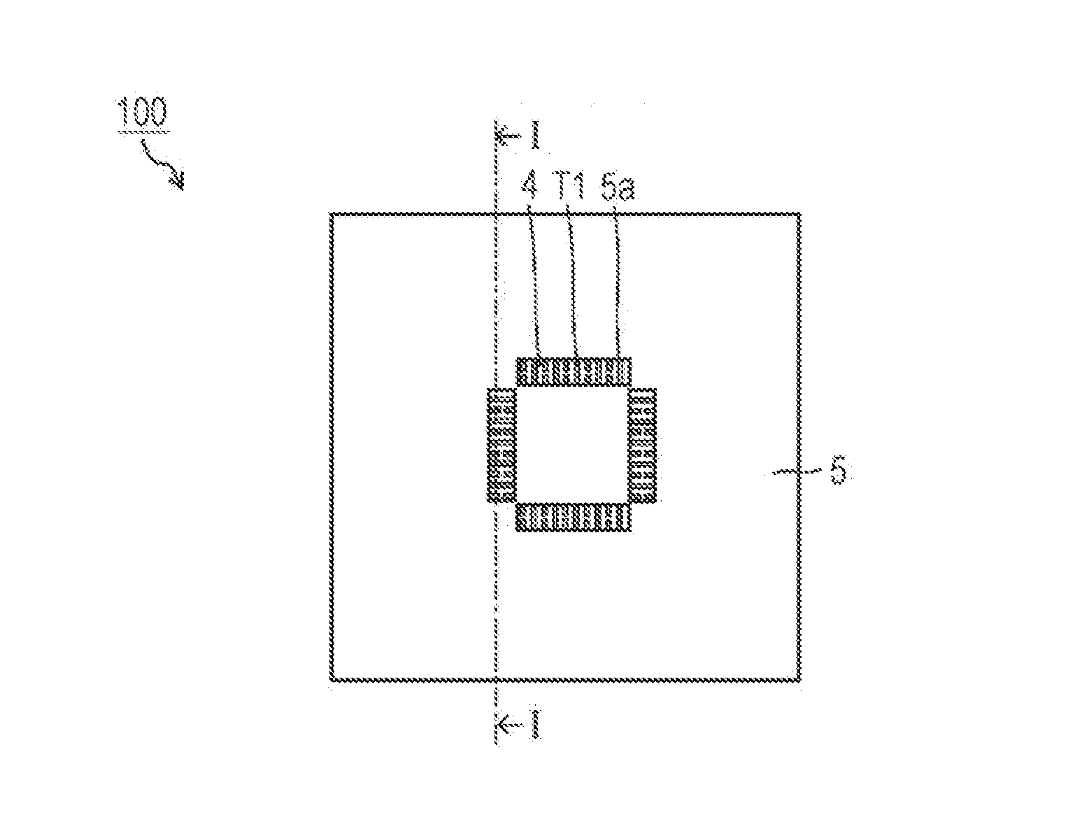
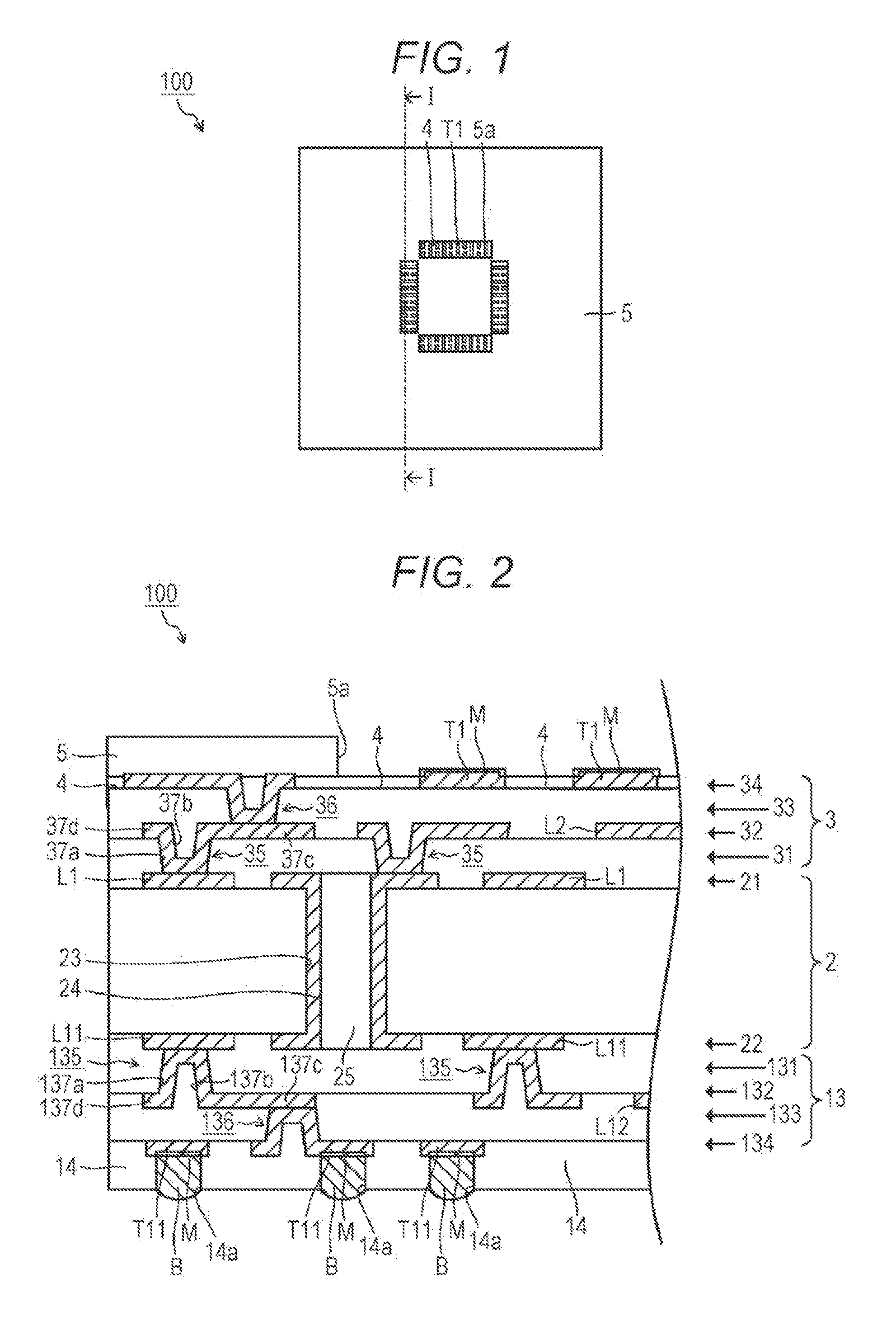
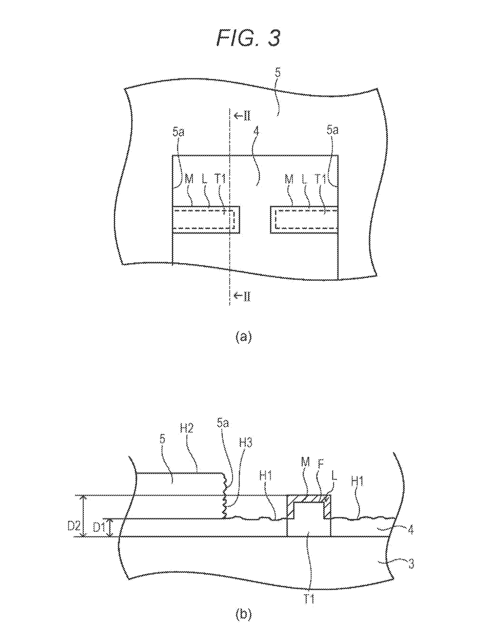
[0032]FIG. 1 is a top view (front face side) of a wiring board 100 according to a first embodiment. FIG. 2 is a partial sectional view of the wiring board 100 taken along the line I-I of FIG. 1. FIG. 3 is a configuration diagram of a connecting terminal T1 on the front face side of the wiring board 100. FIG. 3A is a top view of a connecting terminal T1. FIG. 3B is a sectional view taken along the line II-II of FIG. 3A. In the following description, a side to which a semiconductor chip is connected is referred to as a front face side while a side to which a motherboard, a socket, or a similar member (hereinafter referred to as a motherboard or a similar member) is connected is referred to as a reverse surface side.
(Configuration of Wiring Board 100)
[0033]The wiring board 100 illustrated in FIG. 1 to FIG. 3 includes a core substrate 2, a build-up layer 3 (front face side), a filling member 4, a solder resist layer 5, a build-up layer 13 (reverse surface side), and a solder resist laye...
second embodiment
[0080]FIG. 12 is a top view (front face side) of the wiring board 200 according to the second embodiment. FIG. 13 is a partial sectional view of the wiring board 200 taken along the line I-I of FIG. 12. FIG. 14 is a configuration diagram of the connecting terminal T2 on the front face side of the wiring board 200. FIG. 14A is a top view of the connecting terminal T2. FIG. 14B is a sectional view taken along the line II-II of FIG. 14A. A configuration of the wiring board 200 will now be described with reference to FIG. 12 to FIG. 14, wherein like reference numerals designate corresponding or identical elements with the wiring board 100 described with reference to FIG. 1 to FIG. 3 throughout the embodiments, and the repeated description will be omitted correspondingly.
(Configuration of Front Face Side)
[0081]The wiring board 200 includes a lid plating layer 41 that electrically connects to the core conductor layer 21 on the front face side. The lid plating layer 41 and the conductor la...
working example
[0091]The inventors fabricated two wiring boards A and B by the fabrication methods of the wiring board 100 described with reference to FIG. 4 to FIG. 11. The filling member 4 for the wiring board 100 was filled up by the fourth filling up method described with reference to FIG. 8. The wiring board A and the wiring board B differ in that different materials are used for the filling member 4 and the solder resist layer 5. After fabricating the wiring boards A and B, the inventors mounted the semiconductor chips and checked flowability of the underfills.
[0092]FIG. 16 is an enlarged image of the surface of the wiring board according to the embodiment. FIG. 16A is an enlarged image of the surface H1 of the filling member 4 of the wiring board A. FIG. 16B is an enlarged image of the top surface H2 of the solder resist layer 5 of the wiring board A.
[0093]Next, the inventors measured the surface roughness of the fabricated wiring boards A and B. Table 1 shows surface roughness (Ra) of the ...
PUM
 Abstract
Description
Claims
Application Information
 - R&D Engineer
- R&D Manager
- IP Professional
- Industry Leading Data Capabilities
- Powerful AI technology
- Patent DNA Extraction
Browse by: Latest US Patents, China's latest patents, Technical Efficacy Thesaurus, Application Domain, Technology Topic.
© 2024 PatSnap. All rights reserved.Legal|Privacy policy|Modern Slavery Act Transparency Statement|Sitemap