Metal mesh conductive layer and touch panel having the same

a technology of conductive layer and metal mesh, which is applied in the field of conductive layer, can solve the problems of unavoidable yield control, waste of ito and conductive materials, and difficulty in achieving a simple and green process of ito layer

Inactive Publication Date: 2014-07-17
NANCHANG O FILM TECH CO LTD
View PDF10 Cites 20 Cited by
  • Summary
  • Abstract
  • Description
  • Claims
  • Application Information

AI Technical Summary

Benefits of technology

[0018](1) The electrode lead region of the present invention is provided using mesh design, when it is to be bonded to the flexible printed board, the polymer portion of the mesh can enhance the adhesive force between the pin and the conductive adhesive of the flexible circuit board, thus improving the bonding firmness. The electrode lead region is provided using mesh design, which is the first innovation different from the prior art.
[0019](2) The electrode lead region of the present invention is provided using trench design with a trench width less than 10 μm, which unifies the trench width of the transparent electrode region and the trench width of electrode lead region, thus facilitating the selection of the trench depth, meanwhile facilitating the subsequent unification of process parameters of filling the conductive material, and improving the filling uniformity of the conductive material. The electrode lead region is provided using trench design, which the second innovation different from the prior art.

Problems solved by technology

The conventional manufacturing process is complex and lengthy, so that the yield control has become an unavoidable problem in the current touch screen manufacturing stage.
In addition, the conventional manufacturing process inevitably needs etching, during which lots of ITO and conductive materials are wasted.
Therefore, how to achieve a simple and green process of the ITO layer has become a key technical problem to be solved.
However, the PolyIC® is produced based on conventional printing technology, thus the smallest linewidth can only reach 10 μm.
Larger changes of depth-to-width ratio will cause great difficulty for the silver filling process in the trench.

Method used


Image

  • Metal mesh conductive layer and touch panel having the same
  • Metal mesh conductive layer and touch panel having the same
  • Metal mesh conductive layer and touch panel having the same

Examples


embodiment one

[0031]A conductive layer is provided having an electrode lead region made of regular mesh.

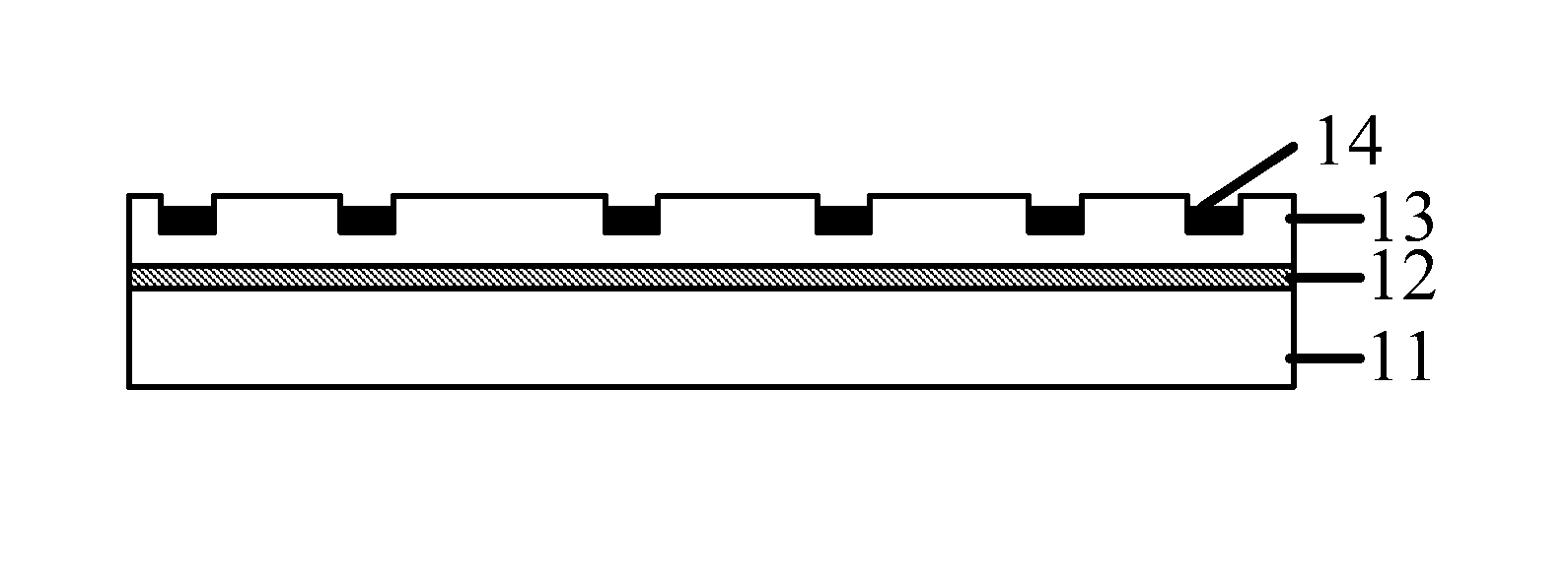
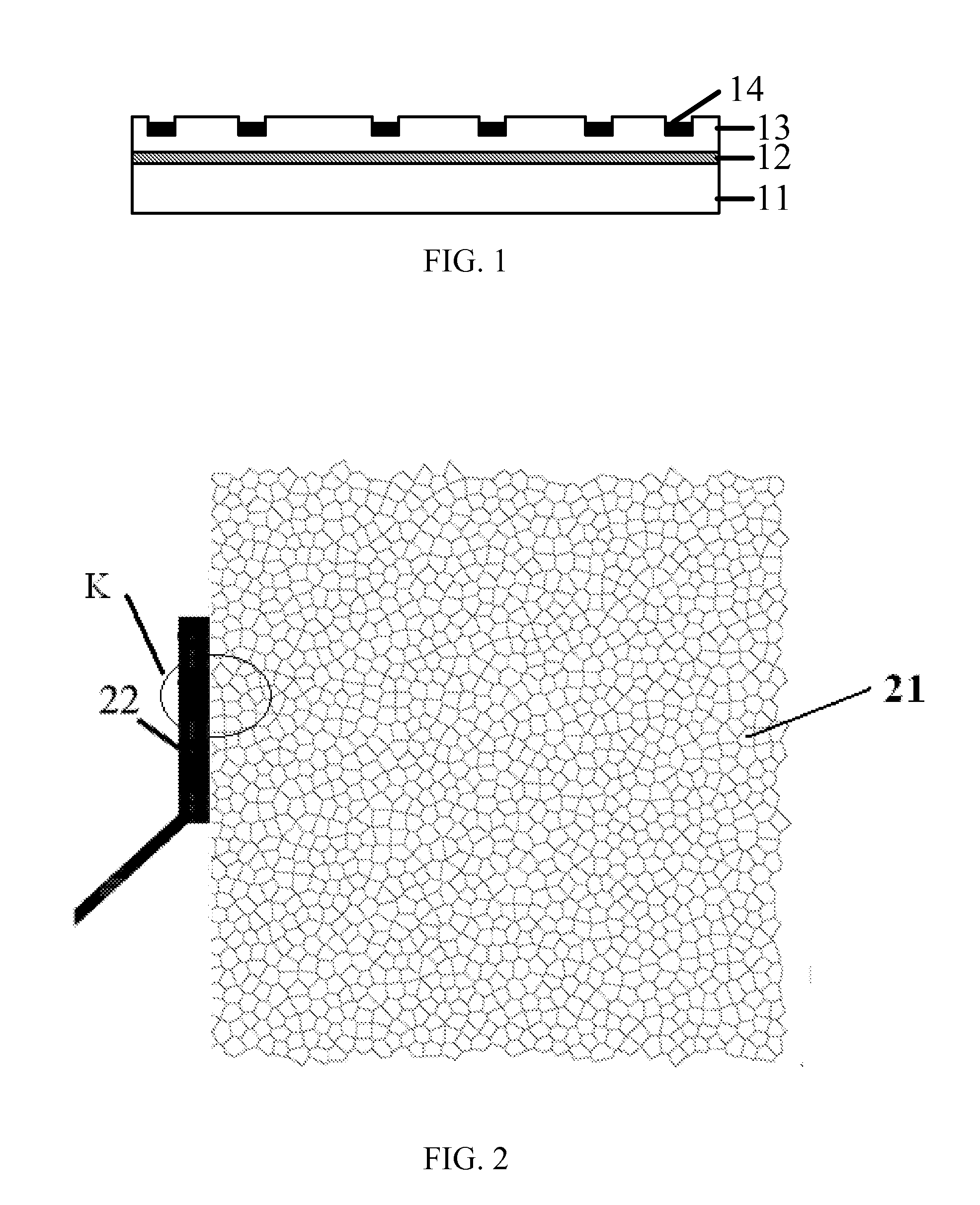
[0032]FIG. 1 is a schematic, cross-sectional view of an embedded metal mesh conductive layer according to an embodiment. The conductive layer includes, bottom-up, a substrate PET 11 with a thickness of 188 μm; a thickening layer 12; and a UV acrylic adhesive 13 having trenches, which has a depth of 3 μm and a width of 2.2 μm. The trench is filled with silver 14 having a thickness of about 2 μm, which is smaller than the depth of the trench.

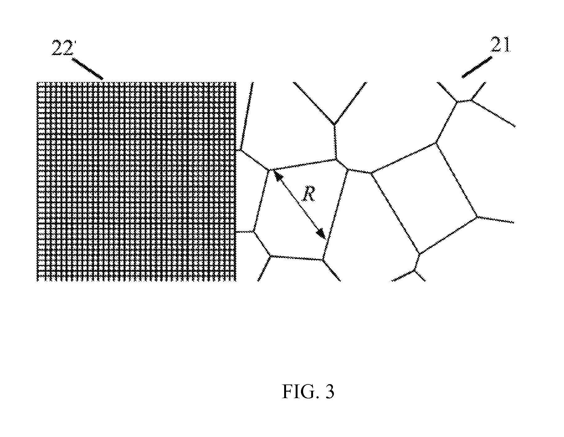
[0033]FIG. 2 is a schematic, plan view of the embedded metal mesh conductive layer according to the present embodiment. The conductive layer includes a transparent electrode region 21 and an electrode lead region 22. The transparent electrode region 21 is composed of a random irregular mesh with a linewidth of 2.2 μm. An average diameter R of the mesh is preferably 120 μm, and the relative transmittance is 96%. Since the selected PET of the present embodimen...


PUM

PropertyMeasurementUnit
angleaaaaaaaaaa
transmittanceaaaaaaaaaa
widthaaaaaaaaaa

Abstract

The present invention relates to to a metal mesh conductive layer and touch panel having the conductive layer. A surface of the conductive layer includes a transparent electrode region and an electrode lead region, the transparent electrode region having a mesh made of metal; the electrode lead region having a mesh made of conductive material containing metal. The mesh is made of conductive material containing metal filled in a trench. The transparent electrode region of present invention uses mesh to more uniformly fill the conductive material into the trench, as well as a better bonding to the outside conductive material. The transparent electrode region made of irregular mesh can prevent the generation of Moire.

Description

FIELD OF THE INVENTION[0001]The present invention relates to conductive layers, and more particularly relates to a metal mesh conductive layer and a touch panel having the conductive layer.BACKGROUND OF THE INVENTION[0002]Touch screen is a sensing device used to receive touch input signals. The touch screen gives a new manner for information exchange and thus it is an attractive whole new information exchange device. The development of the touch screen technology has aroused widespread concern at domestic and foreign information media sector, and it has become a sunrise high-tech industries in the photovoltaic field.[0003]The ITO layer is a crucial component for the touch screen module. Although the manufacturing technology of the touch screen has been rapidly developed, taking the projected capacitive screen as an example, the basic manufacturing process of the ITO layer does not change in recent years. The process inevitably includes the ITO coating, the ITO patterning, and the tr...

Claims


Application Information

Patent Timeline
Patent Type & Authority Applications(United States)
IPC IPC(8): H05K1/11G06F3/041
CPCG06F3/041H05K1/11G06F2203/04112G06F3/04164G06F3/0443G06F3/0446G06F3/044G06F3/047G06F2203/04103
Inventor GAO, YULONGCUI, ZHENGZHANG, SHENG
Owner NANCHANG O FILM TECH CO LTD
Why Eureka
Try Eureka