Eureka AIR delivers breakthrough ideas for toughest innovation challenges, trusted by R&D personnel around the world.

Method of fabricating capacitor structure

Active Publication Date: 2014-07-17
UNITED MICROELECTRONICS CORP
View PDF16 Cites 2 Cited by
  • Summary
  • Abstract
  • Description
  • Claims
  • Application Information

AI Technical Summary

Benefits of technology

The patent text describes a method for forming a hard mask to improve the performance of a MIM capacitor structure. A hard mask material layer is defined using a photo resist pattern, and then the pattern is removed to create a first electrode. This technique helps to minimize or eliminate contaminants caused by the retained photoresist material, which can enhance the performance of the MIM capacitor structure.

Problems solved by technology

However, during the process of fabricating the small-sized MIM capacitor, the MIM capacitor is readily polluted by contaminants.
Under this circumstance, the performance of the MIM capacitor is deteriorated even to the point of breakdown of the MIM capacitor.

Method used


Image

  • Method of fabricating capacitor structure
  • Method of fabricating capacitor structure
  • Method of fabricating capacitor structure

Examples


Embodiment Construction

[0008]The present invention will now be described more specifically with reference to the following embodiments. It is to be noted that the following descriptions of preferred embodiments of this invention are presented herein for purpose of illustration and description only. It is not intended to be exhaustive or to be limited to the precise form disclosed.

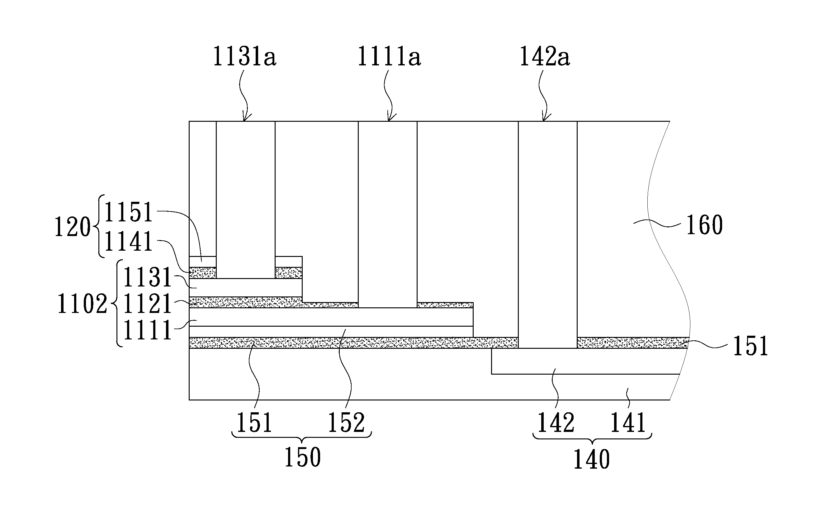
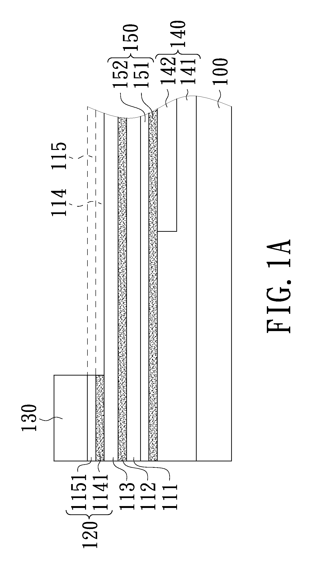
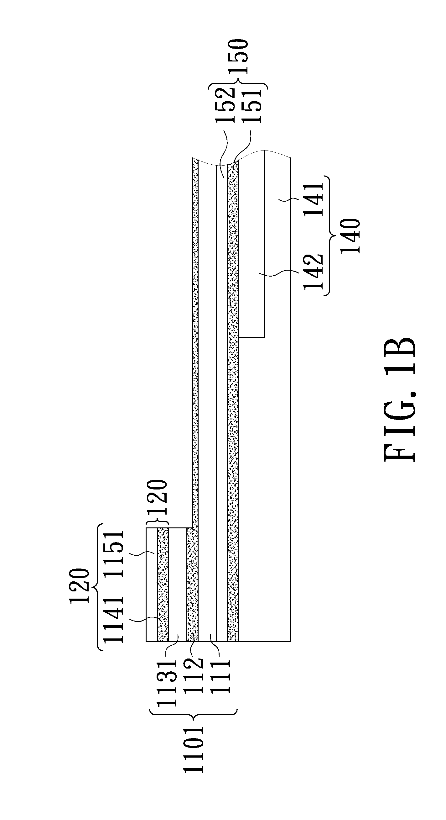
[0009]FIGS. 1A˜1C are schematic cross-sectional views illustrating a method of fabricating a capacitor structure according to an embodiment of the present invention.

[0010]Firstly, as shown in FIG. 1A, a first conductive layer 111, a first insulation layer 112, a second conductive layer 113 and a second insulation layer 114 are sequentially formed over a substrate 100. Then, a hard mask material layer 115 is formed on the second insulation layer 114. Then, a photolithography process is performed to form a photo resist pattern 130 on the hard mask material layer 115. After a portion of the hard mask material layer 115 uncovered by ...


PUM


Abstract

A method of fabricating a capacitor structure includes the following steps. Firstly, a substrate is provided. A first conductive layer, a first insulation layer, a second conductive layer and a second insulation layer are sequentially formed over the substrate. A hard mask material layer is formed on the second insulation layer. Then, the hard mask material layer is defined with a photo resist pattern, so that a hard mask is formed. After the photo resist pattern is removed, the second conductive layer is defined with the hard mask, so that a first electrode of the capacitor structure is formed.

Description

FIELD OF THE INVENTION[0001]The present invention relates to a method of fabricating a semiconductor structure, and more particularly to a method of fabricating a capacitor structure.BACKGROUND OF THE INVENTION[0002]Nowadays, the trends of designing integrated circuits are developed toward miniaturization. As the integration density of the electronic components is increased, the performance of the integrated circuit is enhanced. For example, a metal-insulator-metal (MIM) capacitor and various electronic components are widely used in the high-density integrated circuit. However, during the process of fabricating the small-sized MIM capacitor, the MIM capacitor is readily polluted by contaminants. Under this circumstance, the performance of the MIM capacitor is deteriorated even to the point of breakdown of the MIM capacitor.[0003]Therefore, there is a need of providing an improved MIM capacitor to eliminate the above drawbacks.SUMMARY OF THE INVENTION[0004]In accordance with an aspec...

Claims


Application Information

Patent Timeline
IPC IPC(8): H01L49/02
CPCH01L28/40H01L28/60H01L2924/0002H01L2924/00H01L28/75H01L21/311H01L21/31144H01L23/5223
Inventor CHANG, PAO-CHU
Owner UNITED MICROELECTRONICS CORP
Why Eureka
Eureka Blog
Learn More