

Circuit board and manufacturing method thereof
a technology of circuit board and manufacturing method, which is applied in the field of circuit board, can solve the problems of increasing process complexity and process time, consumption and waste of conductive materials, and achieve the effect of simplifying manufacturing process and process time and manufacturing process
- Summary
- Abstract
- Description
- Claims
- Application Information
AI Technical Summary
Benefits of technology
Problems solved by technology
Method used
Image

Examples
first embodiment
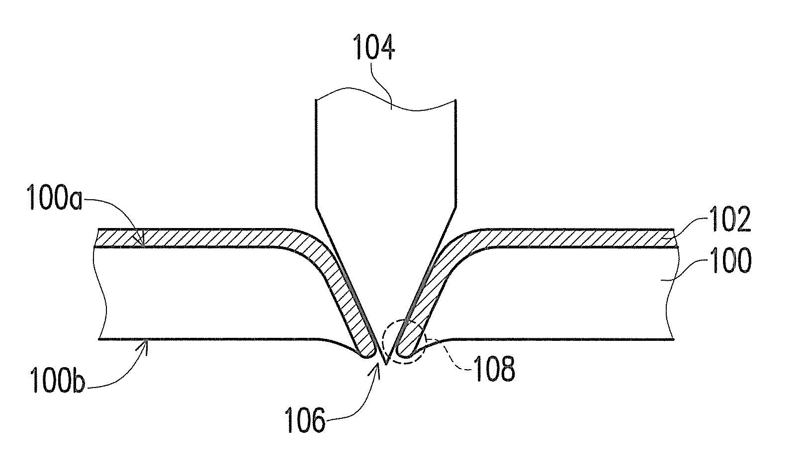
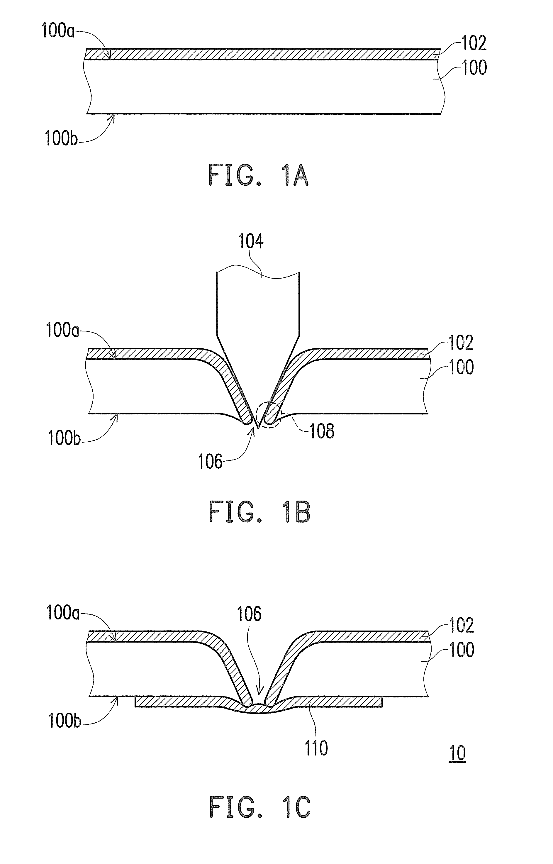
[0024]FIG. 1A through FIG. 1C are cross-sectional views schematically illustrating a manufacturing method of a circuit board according to a first embodiment of the invention. Firstly, referring to FIG. 1A, a substrate 100 is provided. The substrate 100, for example, is a dielectric substrate, which can be a polyethylene tetra phthalate (PET) thin film or a polyimide (PI) thin film. The substrate 100 has a first surface 100a and a second surface 100b opposite to each other. Then, a first circuit layer 102 is formed on the first surface 100a. A material of the first circuit layer 102, for example, is copper or silver. A method for forming the first circuit layer 102, for example, is a printing process. Or, the first circuit layer 102 may also be formed by performing an etching process to a copper foil.
[0025]Next, referring to FIG. 1B, a stress is applied to the first circuit layer 102 and the substrate 100 using a awl tool 104, such that the first circuit layer 102 and the substrate 1...
second embodiment
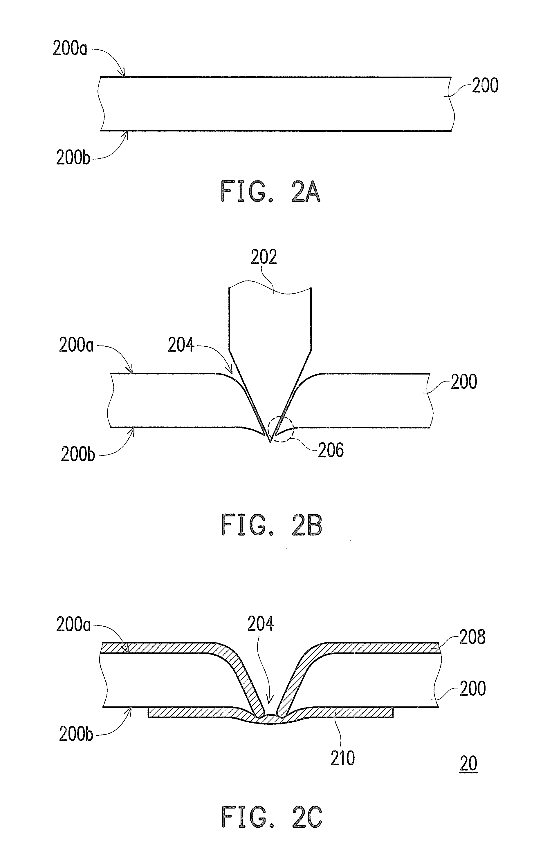
[0029]FIG. 2A through FIG. 2C are cross-sectional views schematically illustrating a manufacturing method of a circuit board according to a second embodiment of the invention. Firstly, referring to FIG. 2A, a substrate 200 is provided. The substrate 200, for example, is a dielectric substrate, which may be a polyethylene tetra phthalate thin film or a polyimide thin film. The substrate 200 has a first surface 200a and a second surface 200b opposite to each other.
[0030]Then, referring to FIG. 2B, a stress is applied to the substrate 200 using a awl tool 202, such that the substrate 200 is deformed to form a through hole 204. The awl tool 202, for example, is a needle. In detail, in this step, the awl tool 202 is used to perforate the substrate 200 so as to form the through hole 204 in the substrate 200.
[0031]Particularly, in the present embodiment, since the awl tool 202 deforms the substrate 200 to form the through hole 204, an end of the resulting through hole 204 neighboring the s...
PUM
| Property | Measurement | Unit |
|---|---|---|
| stress | aaaaa | aaaaa |
| dielectric | aaaaa | aaaaa |
| conductive | aaaaa | aaaaa |
Abstract
Description
Claims
Application Information