Liquid crystal display and manufacturing method thereof
a technology of liquid crystal display and manufacturing method, which is applied in the direction of semiconductor devices, instruments, chemistry apparatus and processes, etc., can solve the problems of disadvantageous affect of liquid crystal display and the inability to essentially eliminate the after-image of methods, so as to improve image quality, reduce the probability of positive and negative ions appearing, and improve conductivity
- Summary
- Abstract
- Description
- Claims
- Application Information
AI Technical Summary
Benefits of technology
Problems solved by technology
Method used
Image
Examples
first embodiment
The First Embodiment
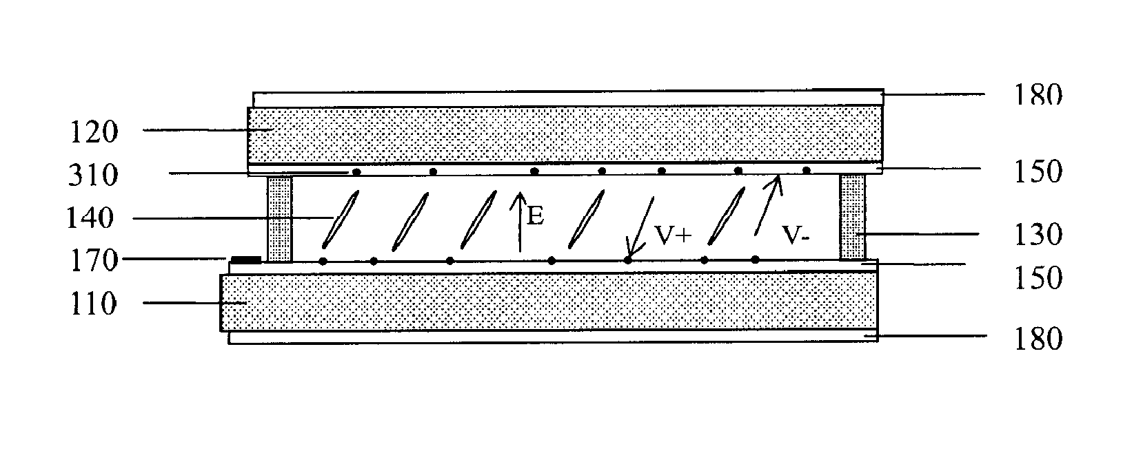
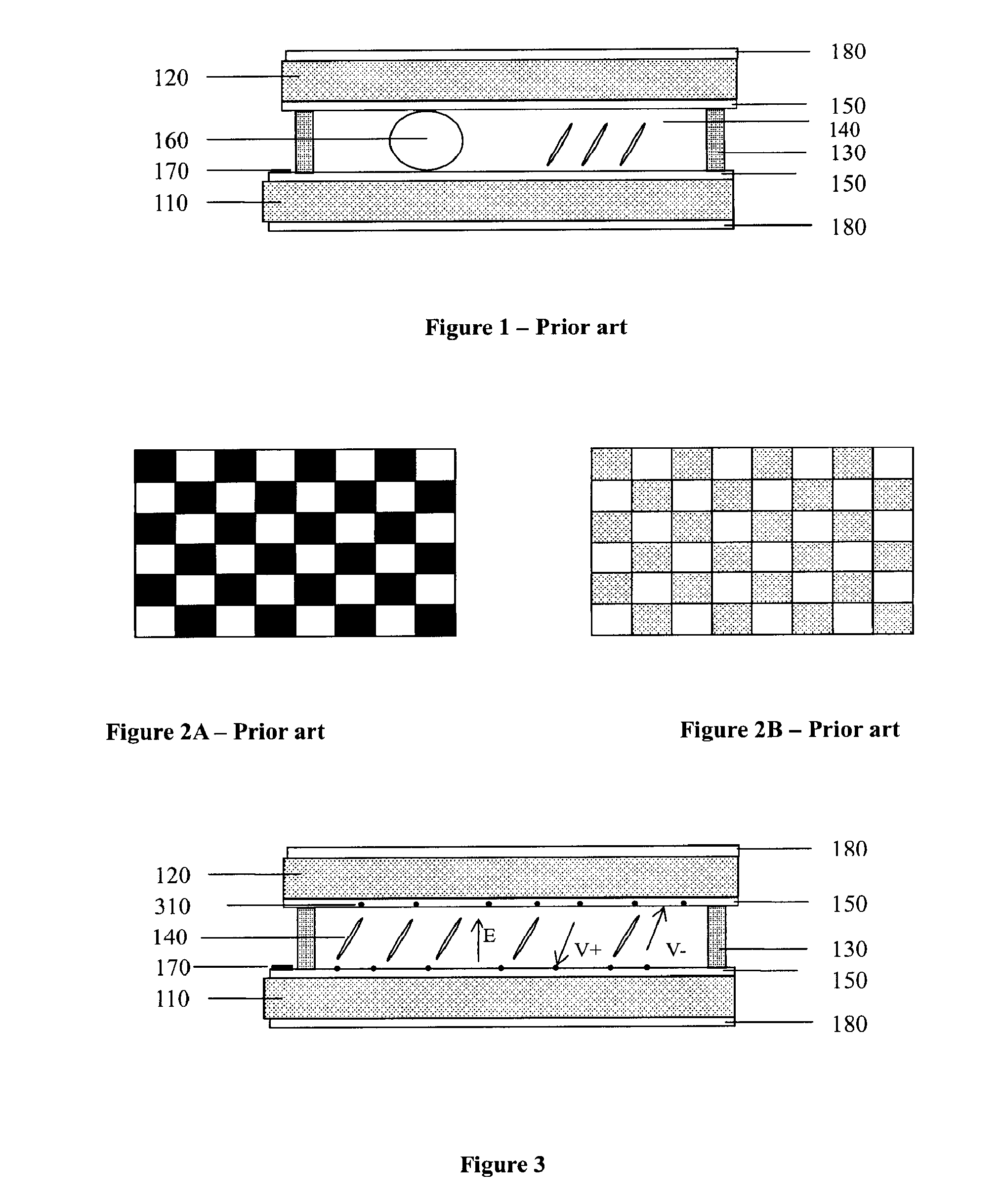
[0028]FIG. 3 is a schematic view of the structure of a LCD according to the first embodiment of the present invention, which illustrates the function of conductive nano-particles.
[0029]As shown in FIG. 3, the LCD according to the first embodiment of the present invention is a thin film transistor liquid crystal display (TFT LCD), such as a transmissive type TFT LCD. The panel of the TFT LCD comprises an array substrate 110 and a color filter substrate 120. The array substrate 110 and the color filter substrate 120 may each comprise a glass substrate and are assembled together by a sealant 130. Between the array substrate 110 and the color filter substrate 120, a dielectric anisotropic liquid crystal layer 140 is provided, one alignment layer 150 is formed on the inner surface of each of the substrates 110 and 120, and spacers 160 are disposed between the substrates 110 and 120. The spacers 160 keep a predetermined spacing between the array substrate 110 and the c...
second embodiment
The Second Embodiment
[0034]Firstly, after the formation of the array substrate 110 and the color filter substrate 120, forming the alignment layers 150 by performing a serial of processes, such as cleaning, coating material of the alignment layer, rubbing, and the like, on the inner side of each of the array substrate 110 and the color filter substrate 120. The thickness of the alignment layers is about 5 nm to about 100 nm.
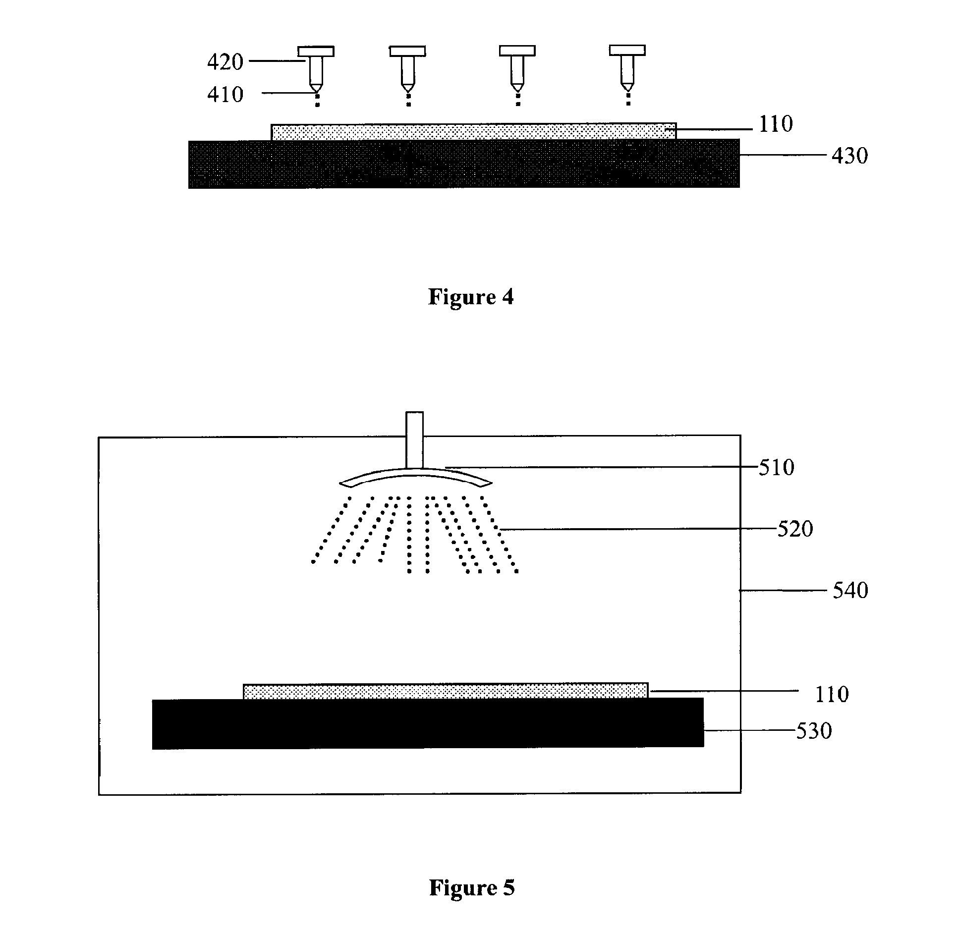
[0035]Then, after cleaning the array substrate 110 and the color filter substrate 120 formed with the alignment layers 150, a mixture solution 410 comprising the conductive nano-particles and the liquid crystal material is dispensed on the alignment layers 150 of the array substrate 110 on a base stage 430 through a nozzle 420 of a liquid crystal dispenser (not shown). The mass ratio of the conductive nano-particles to the liquid crystal ranges from about 0.01:100 to about 0.07:100. FIG. 4 is a schematic view showing dispensing the mixture solution comprising the...
third embodiment
The Third Embodiment
[0037]Firstly, after the formation of the array substrate 110 and the color filter substrate 120, forming the alignment layers 150 by performing a serial of processes, such as cleaning, coating material for the alignment layer, rubbing, and the like, on the inner side of each of the array substrate 110 and the color filter substrate 120. The thickness of the alignment layers is about 50 nm to about 100 nm.
[0038]Then, after cleaning the array substrate 110 and the color filter substrate 120 formed with the alignment layer 150, the array substrate 110 is transported to a base stage 530 of a spherical spacer spraying chamber 540, the mixture 520 of spherical spacers and the conductive nano-particles is sprayed on the surface of the alignment layer of the array substrate 110 through a nozzle of a spherical spacer spraying equipment 510. The mass ratio of the conductive nano-particles to the spherical spacers ranges from about 0.5:100 to about 3.5:100. FIG. 5 is a sch...
PUM
| Property | Measurement | Unit |
|---|---|---|
| diameter | aaaaa | aaaaa |
| thickness | aaaaa | aaaaa |
| thickness | aaaaa | aaaaa |
Abstract
Description
Claims
Application Information


