Chip With Through Silicon Via Electrode And Method Of Forming The Same

a technology of silicon via and electrode, which is applied in the direction of capacitors, semiconductor devices, semiconductor/solid-state device details, etc., can solve the problems of increasing complexity, increasing complexity, and reducing the size of the chip, and achieve the effect of saving manufacturing costs

Active Publication Date: 2014-07-24
UNITED MICROELECTRONICS CORP
View PDF57 Cites 17 Cited by
  • Summary
  • Abstract
  • Description
  • Claims
  • Application Information

AI Technical Summary

Benefits of technology

[0007]The present invention therefore provides a chip with TSV electrode and a method of forming the same, which can save the cost of the processes.
[0010]By forming the TSV electrode and the surface conductive layer simultaneously, the TSV electrode and the surface conductive layer are monolithic, thereby saving the manufacturing cost.

Problems solved by technology

With the development of technology and the increasingly imaginative applications of electrical products, the IC device is becoming smaller, more delicate and more diversified.

Method used


Image

  • Chip With Through Silicon Via Electrode And Method Of Forming The Same
  • Chip With Through Silicon Via Electrode And Method Of Forming The Same
  • Chip With Through Silicon Via Electrode And Method Of Forming The Same

Examples


Embodiment Construction

[0014]To provide a better understanding of the presented invention, preferred embodiments will be described in detail. The preferred embodiments of the present invention are illustrated in the accompanying drawings with numbered elements.

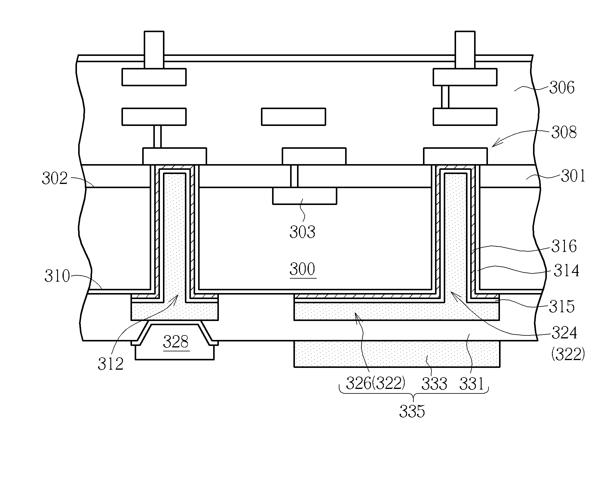
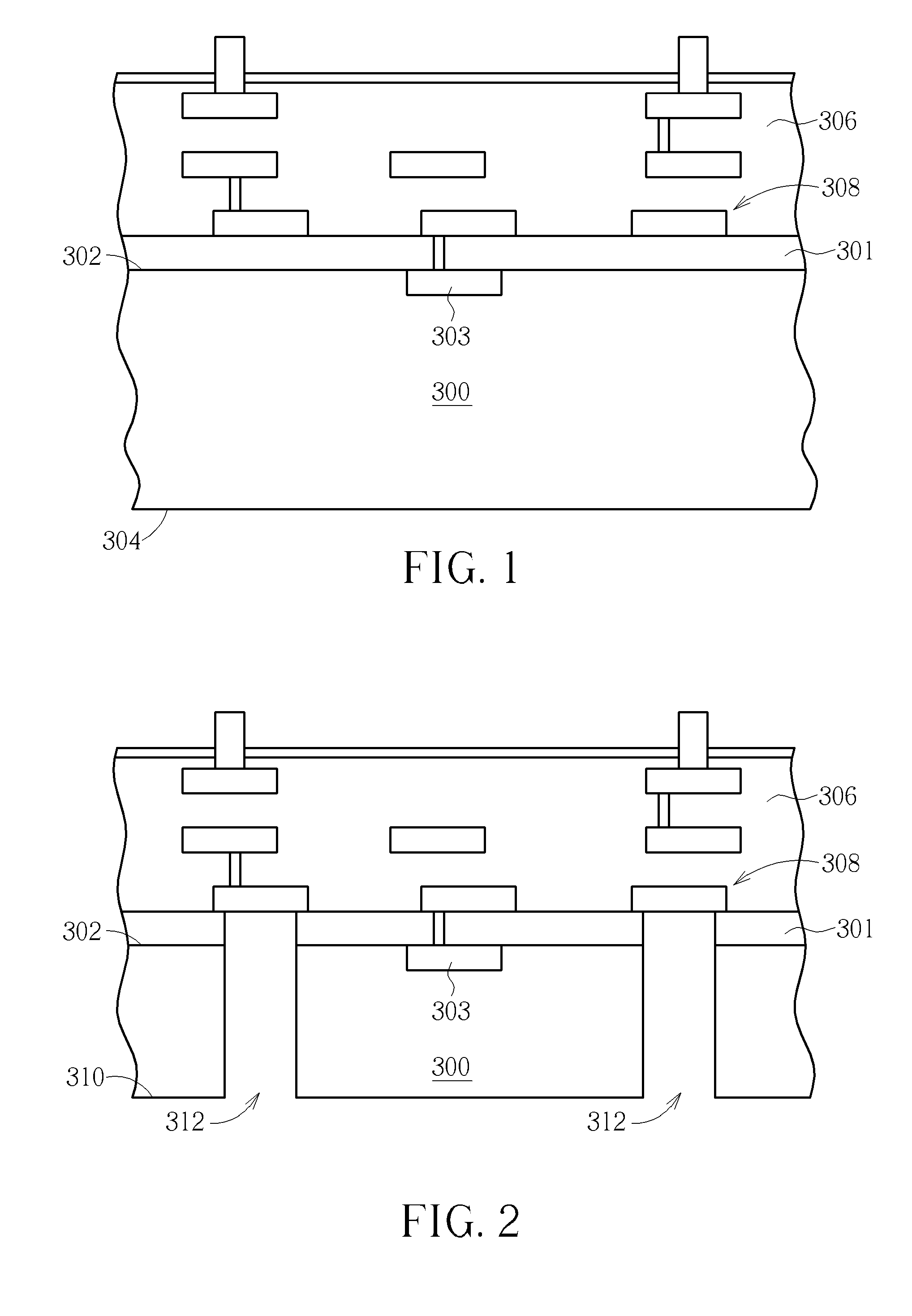
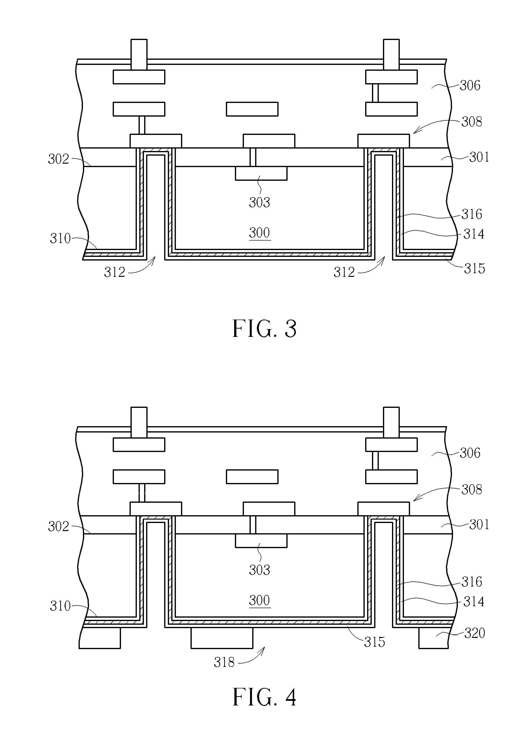
[0015]Please refer to FIG. 1 to FIG. 7, which show schematic diagrams of the method of forming a chip with a TSV electrode according to the first embodiment of the present invention. As shown in FIG. 1, a substrate 300 is provided, such as a silicon substrate, an epitaxial silicon substrate, a silicon germanium substrate, a silicon carbide substrate or a silicon-on-insulator substrate (SOI), but is not limited thereto. The substrate 300 has a first surface 302 and a second surface 304, which are opposite to each other. In one preferred embodiment, the first surface 302 is the active surface of the substrate 300 and the second surface 304 is the back surface of the substrate 300. A thickness of the substrate 300 is about 700 to 1000 micro meters. Nex...


PUM

PropertyMeasurementUnit
conductiveaaaaaaaaaa
surface conductiveaaaaaaaaaa
capacitance densityaaaaaaaaaa

Abstract

The present invention provides a method of forming a chip with TSV electrode. A substrate with a first surface and a second surface is provided. A thinning process is performed from a side of the second surface so the second surface becomes a third surface. Next, a penetration via which penetrates through the first surface and the third surface is formed in the substrate. A patterned material layer is formed on the substrate, wherein the patterned material layer has an opening exposes the penetration via. A conductive layer is formed on the third surface thereby simultaneously forming a TSV electrode in the penetration via and a surface conductive layer in the opening.

Description

BACKGROUND OF THE INVENTION[0001]1. Field of the Invention[0002]The present invention relates to a chip and the forming method thereof, and more particularly, to a chip with a through silicon via (TSV) electrode and the forming method thereof.[0003]2. Description of the Prior Art[0004]In modern society, the micro-processor system comprised of integrated circuits (IC) is a ubiquitous device, being utilized in such diverse fields as automatic control electronics, mobile communication devices and personal computers. With the development of technology and the increasingly imaginative applications of electrical products, the IC device is becoming smaller, more delicate and more diversified.[0005]As is well known in the art, an IC device is produced from dies that are fabricated by conventional semiconductor manufacturing processes. The process to manufacture a die starts with a wafer: first, different regions are marked on the wafer; second, conventional semiconductor manufacture process...

Claims


Application Information

Patent Timeline
Patent Type & Authority Applications(United States)
IPC IPC(8): H01L23/538
CPCH01L28/00H01L23/5384H01L2924/0002H01L28/60H01L23/5226H01L2224/0401H01L21/76898H01L23/481H01L23/49827H01L24/16H01L2225/06541H01L2224/4824H01L2225/06513H01L21/283H01L21/302H01L21/7685H01L21/76865H01L21/76871H01L21/76883H01L24/03H01L2224/02317H01L2924/00
Inventor LIN, MING-TSELIN, CHU-FUKUO, CHIEN-LILIN, YUNG-CHANG
Owner UNITED MICROELECTRONICS CORP
Why Eureka
Try Eureka