

TFT array substrate and manufacturing method thereof and liquid crystal display device
a technology of array substrate and liquid crystal display, which is applied in the direction of semiconductor devices, instruments, electrical devices, etc., can solve the problems of flicker or serious crosstalk in the plane, adversely affecting the picture quality of the panel, and the edge distance of pixels, so as to improve the display effect of the liquid crystal display, reduce the resistance of the common electrode layer, and reduce the manufacturing process. the effect of simple structur
- Summary
- Abstract
- Description
- Claims
- Application Information
AI Technical Summary
Benefits of technology
Problems solved by technology
Method used
Image

Examples
embodiment 1
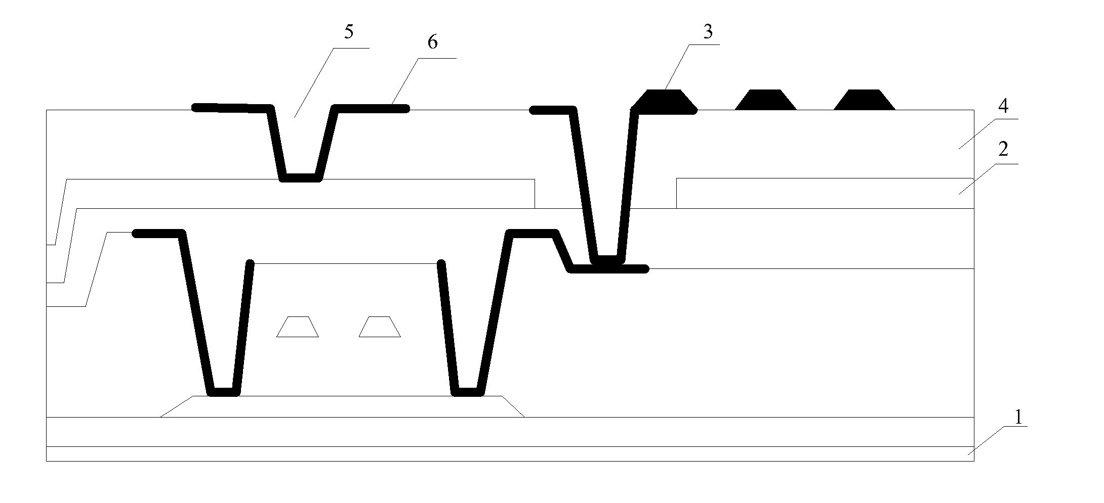
[0022]As illustrated in FIG. 1, an embodiment of the invention provides a TFT array substrate, which mainly includes: a substrate 1, a common electrode layer 2 arranged on the substrate 1, a first insulating layer 4 arranged on the common electrode layer 2 and a plurality of pixel electrodes 3 arranged in an array on the first insulating layer 4, wherein via holes 5 penetrating through the first insulating layer 4 are formed between adjacent pixels in some of a plurality of pixels, and common electrode lines 6 are grown between rows and / or columns of pixels in some of the plurality of pixels, and in parallel with the common electrode layer 2 located below the first insulating layer 4 through the via holes 5.
[0023]A plurality of common electrode lines and a plurality of via holes are arranged on the first insulating layer above the common electrode layer in the embodiment of the invention, and the common electrode lines are in contact with the common electrode layer through the via h...
embodiment 2
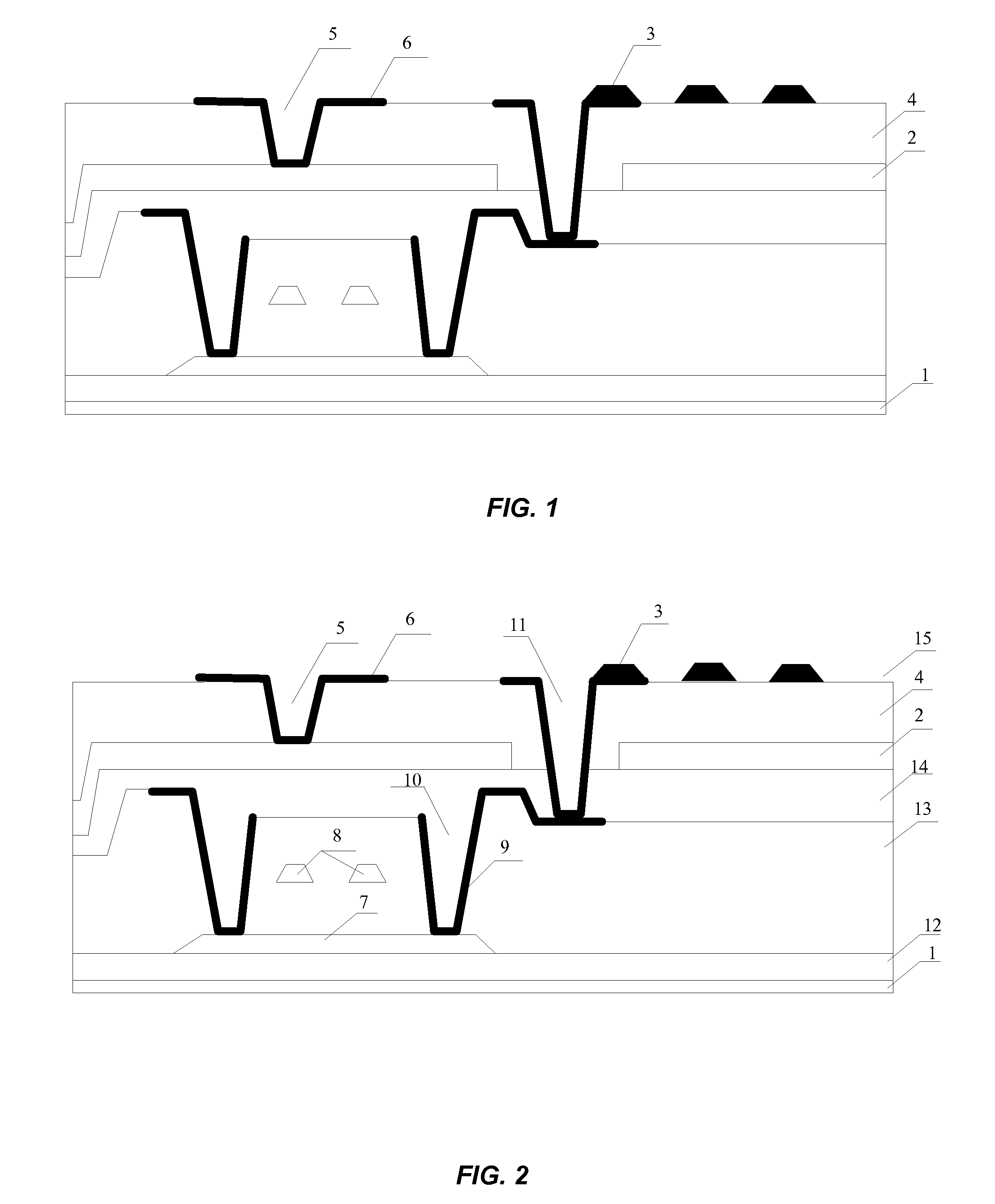
[0056]As illustrated in FIG. 2, the top gate type TFT array substrate can be manufactured as follows.
[0057]A semiconductor structure (e.g., a semiconductor layer 7) of a TFT is formed on a substrate 1. Specifically, a semiconductor active layer made of amorphous silicon (a-Si) may be formed by a chemical vapor deposition process. The amorphous silicon for the semiconductor active layer is merely taken as an example in this embodiment, but the semiconductor active layer is not limited to the amorphous silicon, and in another embodiment, after the semiconductor active layer is formed, an ohmic contact layer on the semiconductor active layer is formed using a chemical vapor deposition process. After exposure, development and etching, the semiconductor active layer or the semiconductor active layer and the ohmic contact layer thereon are patterned to form the semiconductor structure (the semiconductor layer 7) of the TFT.
[0058]A semiconductor insulating layer is formed on the semiconduc...
embodiment 3
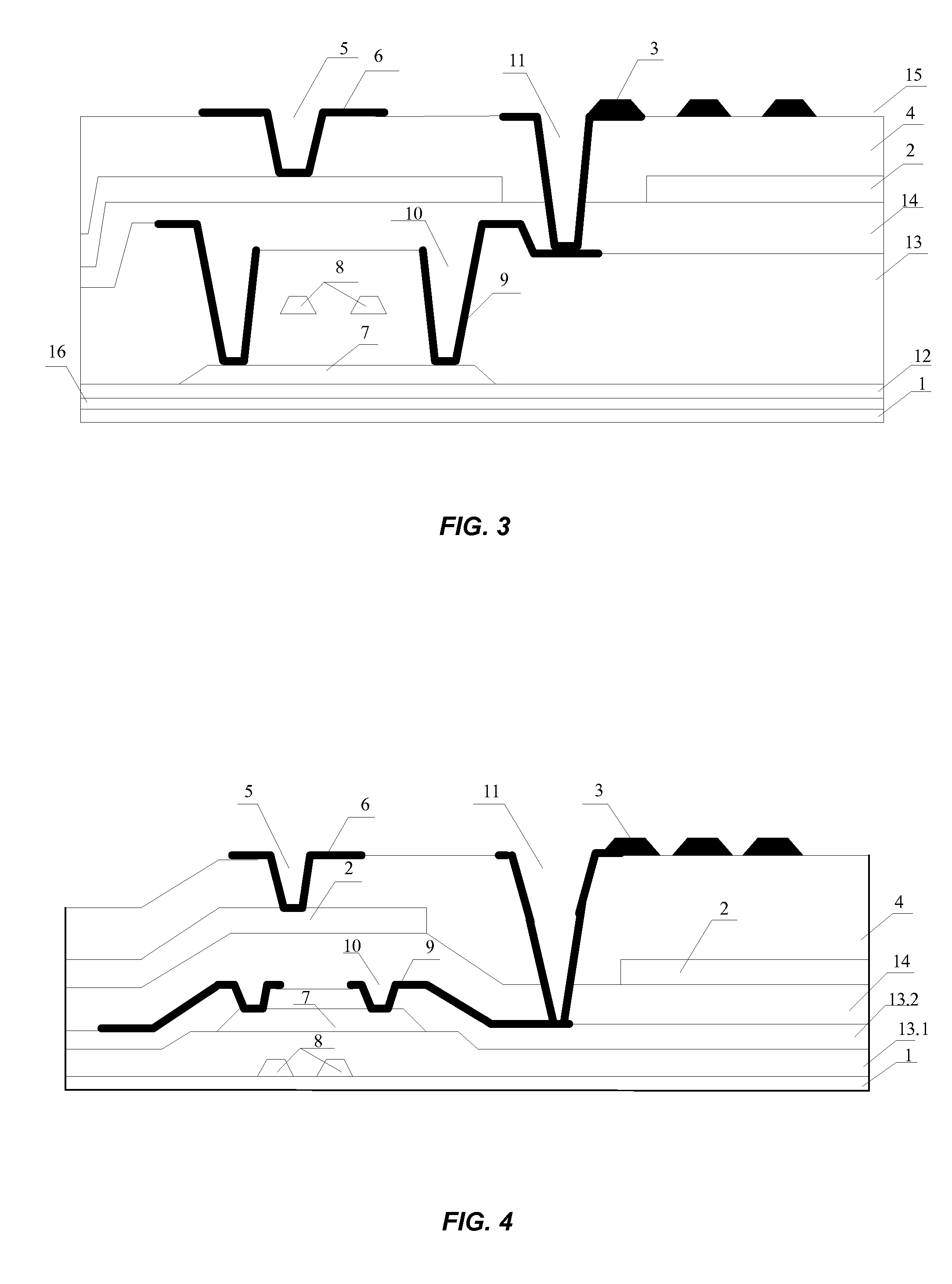
[0066]Referring to FIG. 3, the difference between embodiment 3 and embodiment 2 is that a light shading layer 16 is first formed on the substrate 1 before the semiconductor layer 7 is formed to prevent the TFT array substrate from light leakage. Further, after the light shading layer 16 is formed, a second insulating layer 12 is formed on the substrate 1, to prevent the substrate 1 from polluting the following semiconductor layer 7.
PUM
| Property | Measurement | Unit |
|---|---|---|
| diameter | aaaaa | aaaaa |
| width | aaaaa | aaaaa |
| transparent | aaaaa | aaaaa |
Abstract
Description
Claims
Application Information