Methods of processing substrates

a technology of substrates and processing methods, applied in the direction of lamination ancillary operations, semiconductor devices, chemistry apparatus and processes, etc., can solve the problems of inability to apply high-temperature processes and damage to wafers

Active Publication Date: 2014-07-31
SAMSUNG ELECTRONICS CO LTD
View PDF8 Cites 24 Cited by
  • Summary
  • Abstract
  • Description
  • Claims
  • Application Information

AI Technical Summary

Benefits of technology

[0006]Exemplary embodiments of the present general inventive concept provide methods of processing substrates in which a carrier can be bonded to the wafer with thermal stability.

Problems solved by technology

UV radiation is applied to the glue layer in order to use the UV curable adhesive, but the wafer can be damaged from the UV radiation.
If instead a thermoplastic adhesive is adopted as the glue layer, a high temperature process cannot be applied due to poor thermal stability of the adhesive.

Method used


Image

  • Methods of processing substrates
  • Methods of processing substrates
  • Methods of processing substrates

Examples


Embodiment Construction

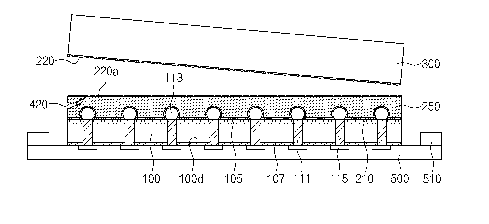
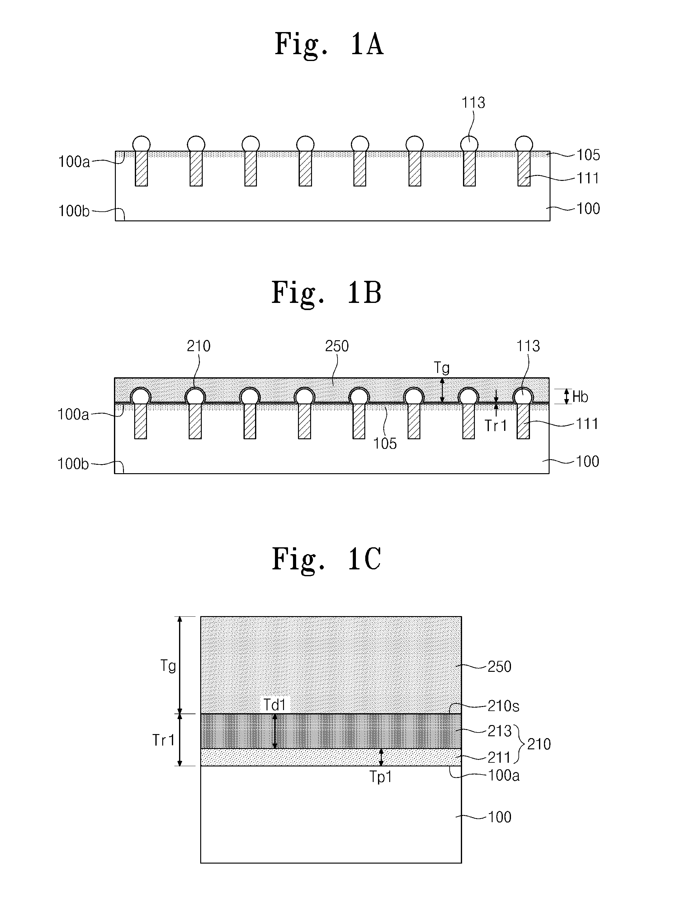
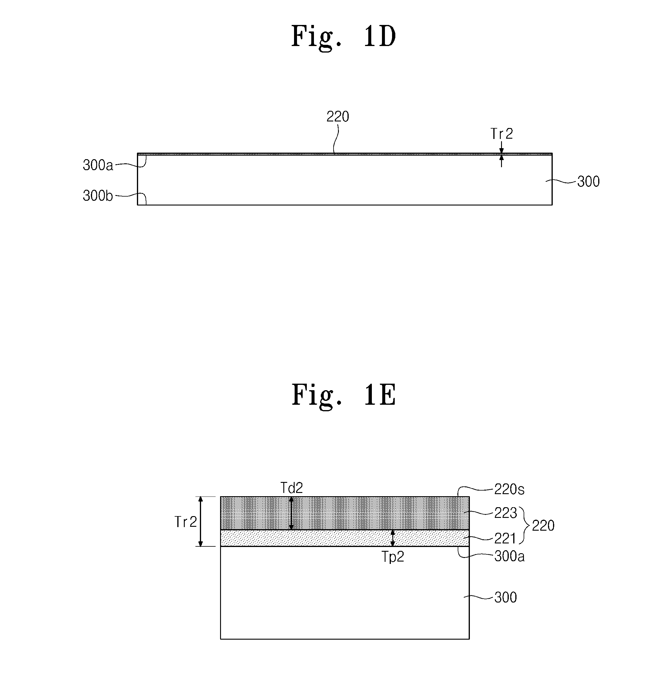
[0042]Example embodiments of inventive concepts will now be described more fully hereinafter with reference to the accompanying drawings, in which some example embodiments of inventive concepts are shown. Example embodiments, may, however, be embodied in many different forms and should not be construed as being limited to the embodiments set forth herein. Rather, these example embodiments are provided so that this disclosure will be thorough and complete, and will fully convey the scope of exemplary embodiments of inventive concepts to those of ordinary skill in the art. In the drawings, the thicknesses of layers and regions are exaggerated for clarity. Like reference numerals in the drawings denote like elements. Hereinafter, exemplary embodiments of the present general inventive concept will be described with reference to the accompanying drawings. The drawings are not necessarily to scale, emphasis instead being placed upon illustrating the principles of the present general inven...


PUM

PropertyMeasurementUnit
thickness Tr1aaaaaaaaaa

Abstract

Methods processing substrates are provided. The method may include providing a bonding layer between a substrate and a carrier to bond the substrate to the carrier, processing the substrate while the substrate is supported by the carrier, and removing the bonding layer to separate the substrate from the carrier. The bonding layer may include a thermosetting glue layer and thermosetting release layers provided on opposing sides of the thermosetting glue layer.

Description

CROSS-REFERENCE TO RELATED APPLICATIONS[0001]This U.S. nonprovisional patent application claims priority under 35 U.S.C. §119(a) from Korean Patent Application 10-2013-0008695 filed on Jan. 25, 2013, the entire contents of which are hereby incorporated by reference.BACKGROUND OF THE INVENTION[0002]1. Field of the Invention[0003]The present inventive concept relates to methods of processing substrates and, more particularly, to methods of thinning wafers.[0004]2. Description of the Related Art[0005]In a process of manufacturing a semiconductor, a wafer is bonded to a carrier with glue and release layers therebetween in order to thin the wafer by a back lap process. An ultraviolet (UV) curable adhesive is generally used as the glue layer. UV radiation is applied to the glue layer in order to use the UV curable adhesive, but the wafer can be damaged from the UV radiation. If instead a thermoplastic adhesive is adopted as the glue layer, a high temperature process cannot be applied due ...

Claims


Application Information

Patent Timeline
Patent Type & Authority Applications(United States)
IPC IPC(8): H01L21/683H01L21/302
CPCH01L21/6835H01L21/6836H01L2221/68318H01L21/02057H01L2221/6834H01L2221/68381H01L21/302H01L2221/68327H01L24/03H01L24/13H01L24/16H01L24/17H01L24/92H01L24/94H01L2224/03002H01L2224/036H01L2224/0401H01L2224/13025H01L2224/16145H01L2224/16146H01L2224/16227H01L2224/17181H01L2224/92H01L2224/9222H01L2224/92222H01L2224/94H01L2225/06513H01L2225/06517H01L2225/06541H01L2225/06565H01L2924/15311H01L2224/11H01L2224/03H01L2924/00014H01L2221/68304H01L21/304H01L2221/68368H01L21/78H01L2224/81H01L21/02H01L21/20
Inventor LEE, CHUNGSUNKIM, JUNG-HWANCHOI, KWANG-CHULKANG, UN-BYOUNGLEE, JEON IL
Owner SAMSUNG ELECTRONICS CO LTD
Why Eureka
Try Eureka