Conductive component and preparation method thereof
a technology of conductive components and components, applied in the field of conductive components, can solve the problems of high cost of conductive components
- Summary
- Abstract
- Description
- Claims
- Application Information
AI Technical Summary
Benefits of technology
Problems solved by technology
Method used
Image

Examples
Embodiment Construction
[0048]Reference will now be made to the drawings to describe, in detail, embodiments of the present conductive component and a preparation method thereof
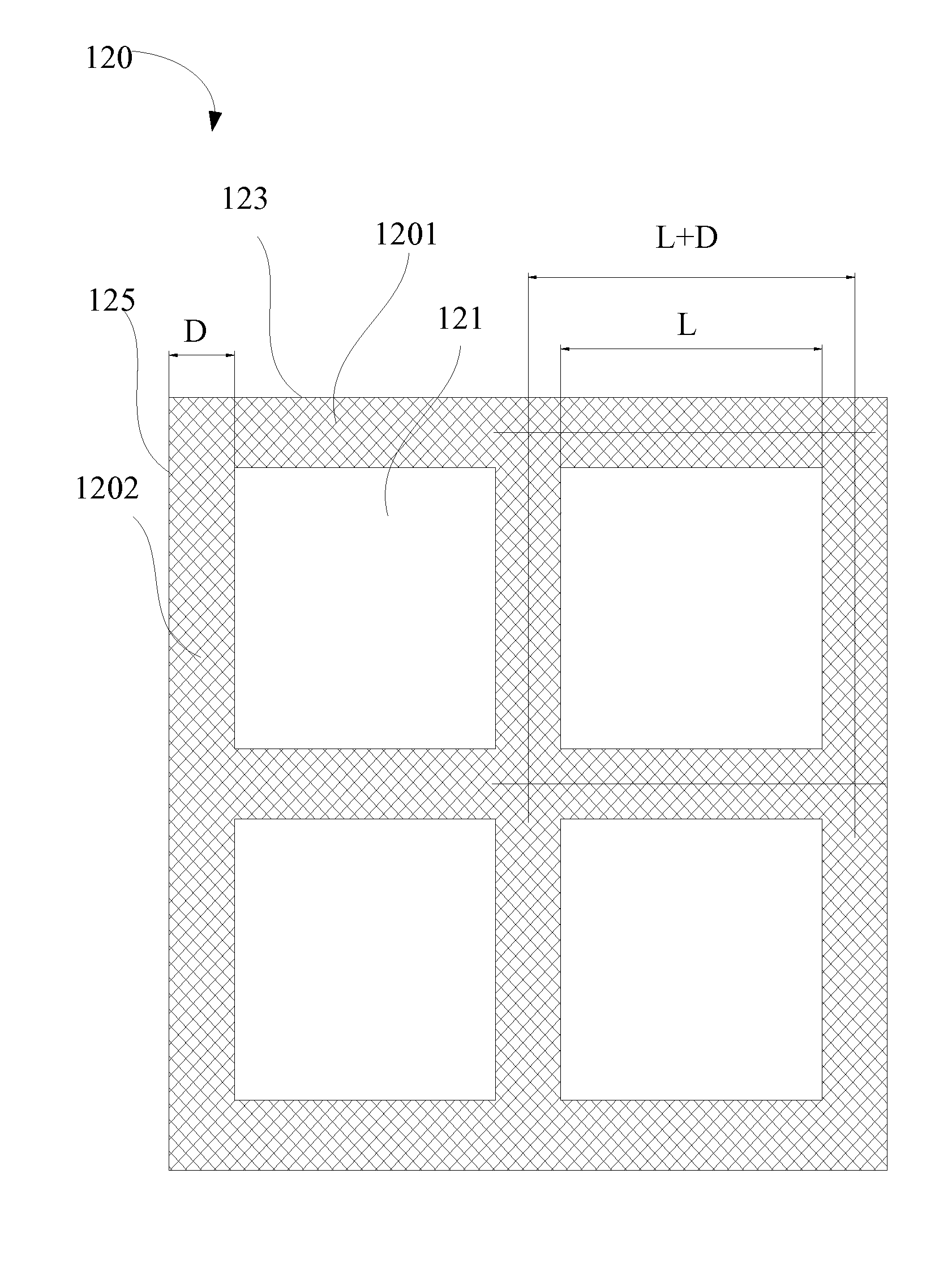
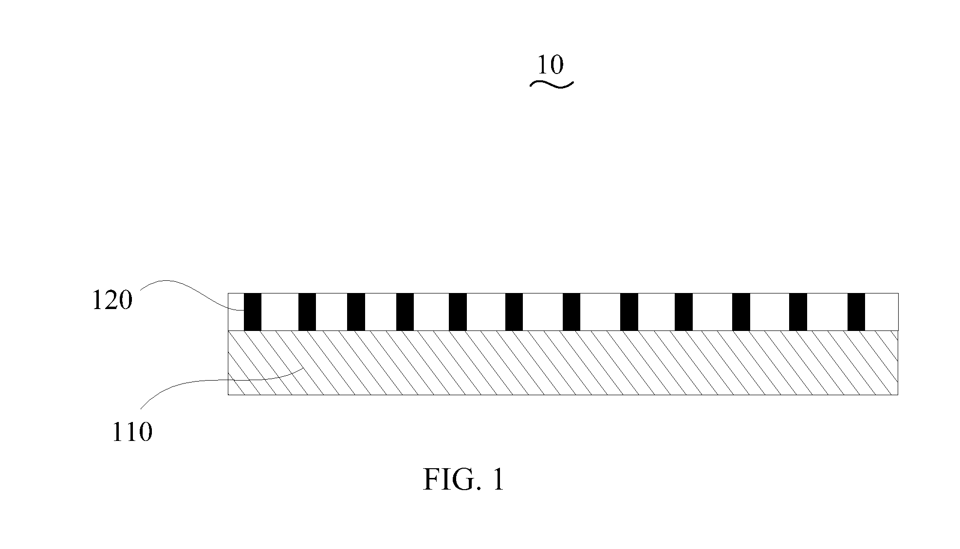
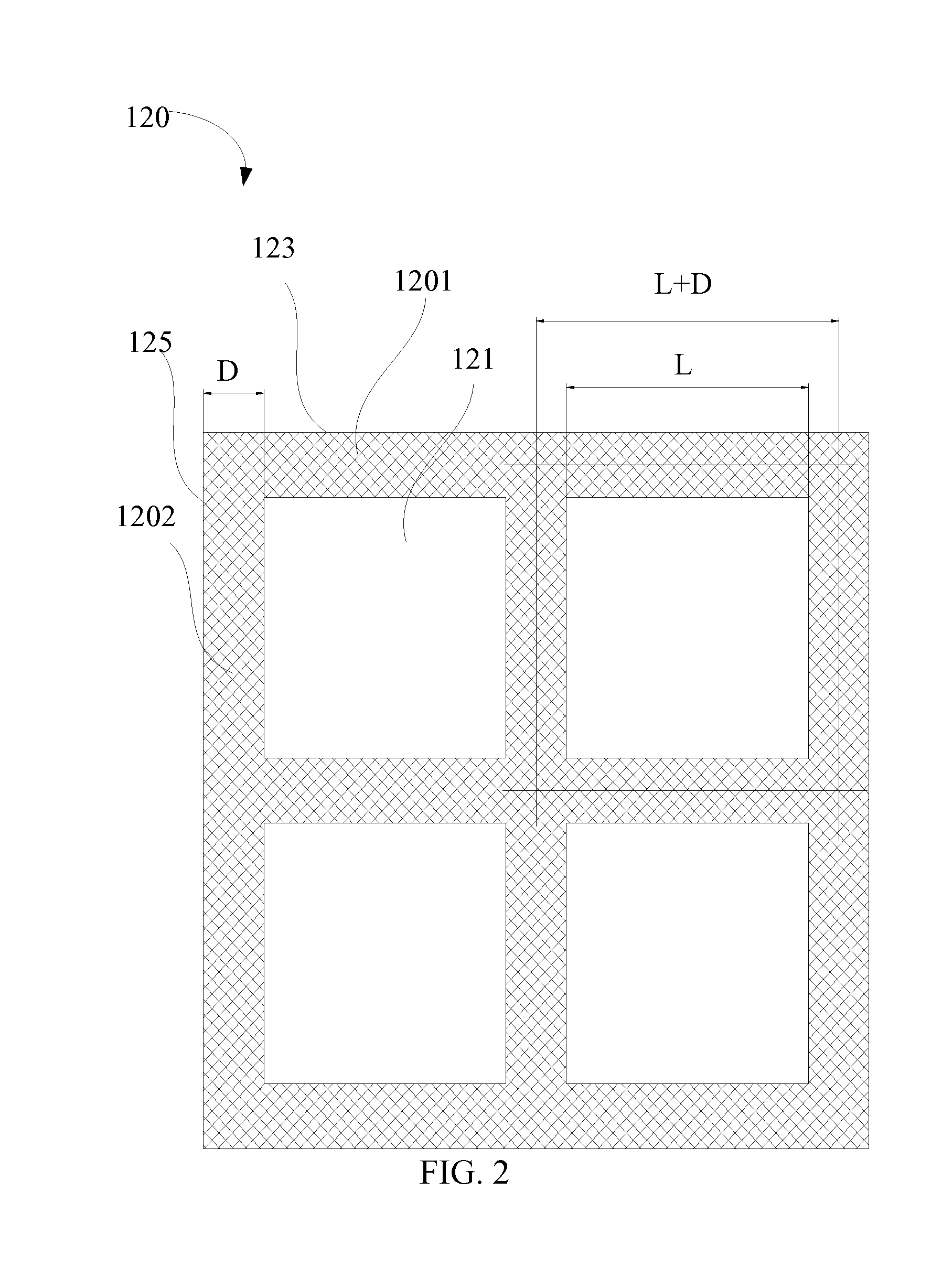
[0049]Referring to FIG. 1, an embodiment of a conductive component 10 includes an insulating layer 110 and a metal mesh 120 arranged on the insulating layer 110.
[0050]The insulating layer 110 is a glass substrate or a plastic film. The glass substrate is made of a material of inorganic silicate or polymethyl methacrylate (PMMA). The plastic film is made of a material of polyethylene terephthalate (PET) or polycarbonate (PC). In a word, the insulating layer 110 is made of transparent insulating material.
[0051]The insulating layer 110 is substantially sheet-like. The surface of the insulating layer 110 is provided with a functional layer having functions of anti-dazzle, hardening, antireflection and atomization (not shown). Where, the functional layer having the functions of anti-dazzle or atomization is formed by coating a paint havi...
PUM
| Property | Measurement | Unit |
|---|---|---|
| widths | aaaaa | aaaaa |
| widths | aaaaa | aaaaa |
| thickness | aaaaa | aaaaa |
Abstract
Description
Claims
Application Information