Organic electroluminescence element

a technology of electroluminescence element and organic el, which is applied in the direction of luminescent composition, organic chemistry, chemistry apparatus and processes, etc., can solve the problems high efficiency of phosphorescent organic el device cannot be obtained by merely applying fluorescent device technology, and hydrocarbon-based compound is hardly selected, so as to achieve high luminous efficiency and long life

Inactive Publication Date: 2014-08-07
IDEMITSU KOSAN CO LTD
View PDF13 Cites 30 Cited by
  • Summary
  • Abstract
  • Description
  • Claims
  • Application Information

AI Technical Summary

Benefits of technology

[0249]In the organic EL device of the invention, it is preferred that a layer comprising a compound represented by the following formula (10) be bonded to the anode. This compound has a strong accepter property and hence, due to the provision of this layer, the amount of holes injected to the emitting layer is further increased. In the device in which the amount of injected holes is large, the configuration of the invention exhibits further significantly advantageous effects.
[0250]In the formula, R11 to R16 are independently a cyano group, —CONH2, a carboxy group or —COOR17 (R17 is an alkyl group including 1 to 20 carbon atoms), or R11 and R12, R13 and R14 or R15 and R16 are bonded with each other to form —CO—O—CO—.
[0251]As the alkyl group including 1 to 20 carbon atoms represented by R17, a linear or branched alkyl group can be given. Specifically, a methyl group, an ethyl group, a propyl group, an isopropyl group, an n-butyl group, an isobutyl group, a sec-butyl group, a tert-butyl group, an n-pentyl group, an n-hexyl group, an n-heptyl group, an n-octyl group or the like can be given. A methyl group, an ethyl group, a propyl group, an isopropyl group, an n-butyl group, an isobutyl group, a sec-butyl group and a tert-butyl group are preferable.
[0253]In the organic EL device of the invention, other configurations of the first organic thin film layer and the second organic thin film layer as mentioned above are not particularly restricted, and known materials or the like can be used. Hereinbelow, a brief explanation will be made on the layer of the device according to the embodiment 1. However, materials to be applied to the organic EL device of the invention are not limited to those mentioned below.[Substrate]
[0254]As the substrate, a glass sheet, a polymer sheet or the like can be used.
[0255]Examples of materials of the glass sheet include soda lime glass, barium-strontium-containing glass, lead glass, aluminosilicate glass, borosilicate glass, barium borosilicate glass, quartz, and the like. Examples of materials of the polymer sheet include polycarbonate, acryl, polyethylene terephthalate, polyethersulfone, polysulfone, and the like.[Anode]

Problems solved by technology

It is known that a highly efficient phosphorescent organic EL device cannot be obtained by merely applying fluorescent device technology due to the emission characteristics.
Therefore, in a phosphorescent organic EL device, such a hydrocarbon-based compound is hardly selected.
As a result, an organic compound including a hetero atom such as oxygen and nitrogen is selected, and hence a phosphorescent organic EL device has a problem that it has a short lifetime as compared with a fluorescent organic EL device.

Method used


Image

  • Organic electroluminescence element
  • Organic electroluminescence element
  • Organic electroluminescence element

Examples


embodiment 1

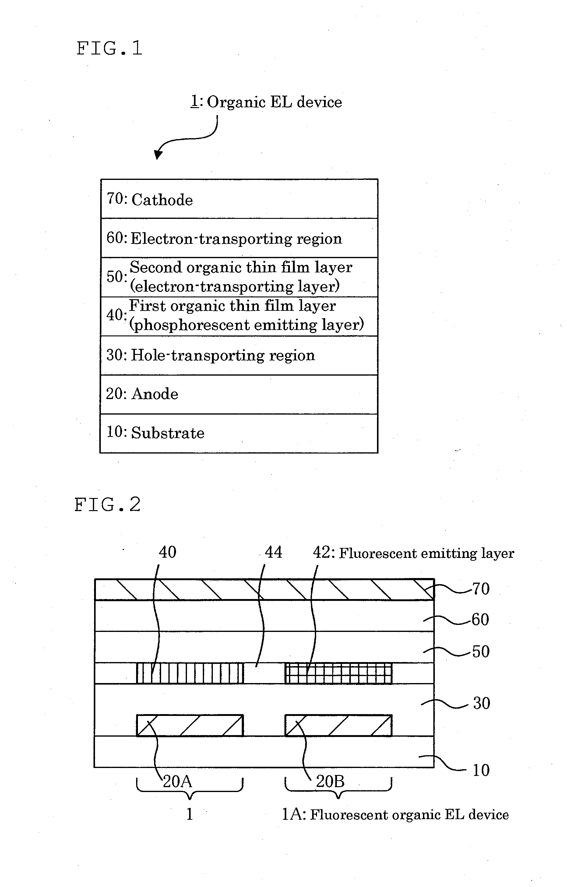
[0227]FIG. 1 is a schematic view showing the layer configuration of the organic EL device of the invention.

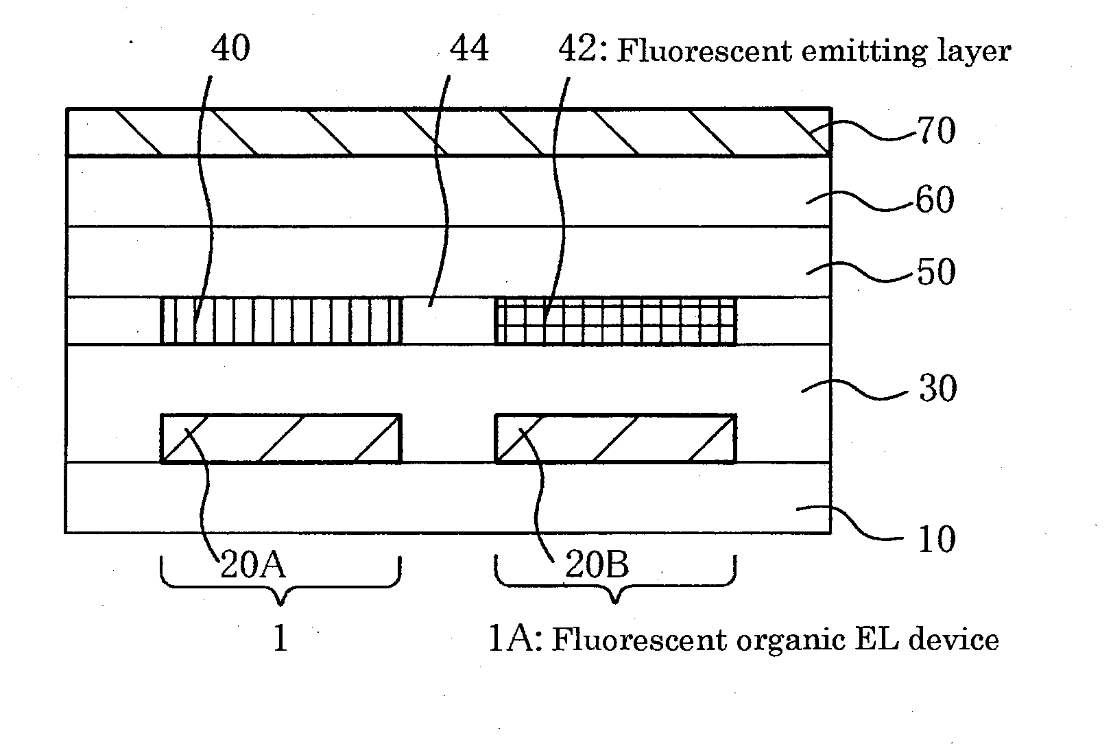
[0228]An organic EL device 1 has a configuration in which an anode 20, a hole-transporting region 30, a first organic thin film layer 40, a second organic thin film layer 50, an electron-transporting region 60 and a cathode 70 are stacked on a substrate 10 in this sequence. The hole-transporting region 30 means a hole-transporting layer, a hole-injecting layer or the like. Similarly, the electron-transporting region 60 means an electron-transporting layer or an electron-injecting layer or the like. They are not required to be formed. However, it is preferred that one or more of these layers be formed.

[0229]In the organic EL device 1, the first organic thin film layer 40 functions as a phosphorescent emitting layer, and the second organic thin film layer 50 functions as an electron-transporting layer and a hole-barrier layer.

[0230]When the first organic thin film layer 40 and th...

embodiment 2

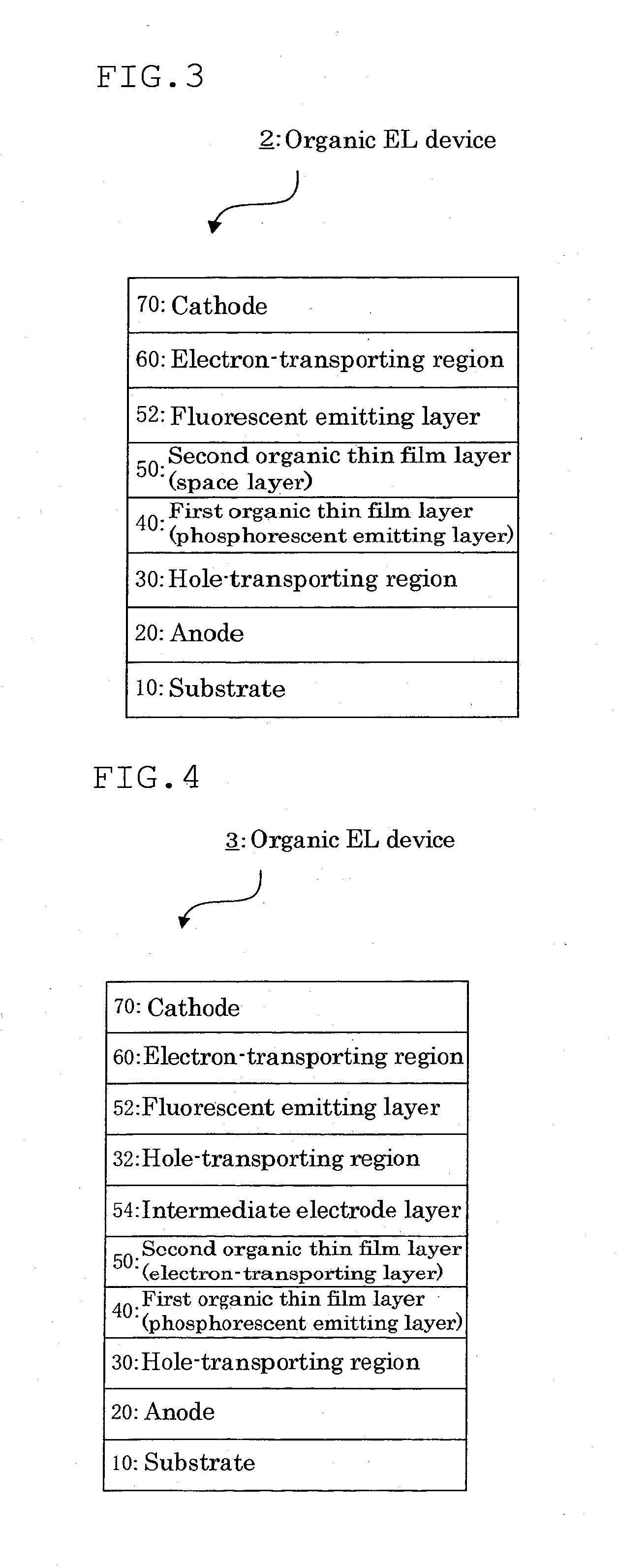
[0239]FIG. 3 is a schematic cross-sectional view showing the layer configuration of an organic EL device according to another embodiment of the invention.

[0240]An organic EL device 2 is an example of a hybrid-type organic EL device in which a phosphorescent emitting layer and a fluorescent emitting layer are stacked.

[0241]The organic EL device 2 has the same configuration as that of the above-mentioned organic EL device 1, except that a fluorescent emitting layer 52 is formed between the second organic thin film layer 50 and the electron-transporting region 60. In the organic EL device 2, the first organic thin film layer 40 functions as a phosphorescent emitting layer and the second organic thin film layer 50 functions as a space layer. In a configuration in which the phosphorescent emitting layer and the fluorescent emitting layer are stacked, in order to prevent excitons formed in the phosphorescent emitting layer from being diffused to the fluorescent emitting layer, there is a ...

embodiment 3

[0243]FIG. 4 is a schematic cross-sectional view showing the layer configuration of an organic EL device according to another embodiment of the invention.

[0244]An organic EL device 3 is an example of a tandem-type organic EL device in which a phosphorescent emitting layer and a fluorescent emitting layer are stacked through an intermediate electrode.

[0245]The organic EL device 3 has a configuration in which the anode 20, the hole-transporting region 30, the first organic thin film layer 40, the second organic thin film layer 50, an intermediate electrode layer 54, a hole-transporting region 32, a fluorescent emitting layer 52, the electron-transporting region 60 and a cathode 70 are stacked in this sequence on the substrate 10. A region disposed between the anode 20 and the intermediate electrode layer 54 is a first emitting unit (phosphorescent emission) and a region disposed between the intermediate electrode layer 54 and the cathode 70 is a second emitting unit (phosphorescent em...


PUM

PropertyMeasurementUnit
ionization potentialaaaaaaaaaa
triplet energyaaaaaaaaaa

Abstract

An organic electroluminescence device including an anode and a cathode being opposed, wherein a first organic thin film layer and a second organic thin film layer are provided between the anode and the cathode sequentially from the anode side; the first organic thin film layer including an aromatic heterocyclic derivative A represented by the following formula (1-1) and a phosphorescent emitting material; and the second organic thin film layer including an aromatic heterocyclic derivative B represented by the following formula (2-1):

Description

TECHNICAL FIELD[0001]The invention relates to an organic electroluminescence device.BACKGROUND ART[0002]An organic electroluminescence (EL) device includes a fluorescent organic EL device or a phosphorescent organic EL device, and a device design optimum for the emission mechanism of each type of organic EL device has been studied. It is known that a highly efficient phosphorescent organic EL device cannot be obtained by merely applying fluorescent device technology due to the emission characteristics. The reasons therefor are generally considered to be as follows.[0003]Specifically, since phosphorescence emission utilizes triplet excitons, a compound used for forming an emitting layer must have a large energy gap. This is because the energy gap (hereinafter often referred to as “singlet energy”) of a compound is normally larger than the triplet energy (in the invention, the difference in energy between the lowest excited triplet state and the ground state) of the compound.[0004]In ...

Claims


Application Information

Patent Timeline
Patent Type & Authority Applications(United States)
IPC IPC(8): H01L51/00
CPCH01L51/0072H01L51/0071C07D403/10C07D487/04C07D491/048C07D519/00C09K11/06C09B57/00C09B57/007C09K2211/1007C09K2211/1011C09K2211/1029C09K2211/1044C09K2211/1059C09K2211/1088C09K2211/1096H10K59/32H10K85/633H10K85/342H10K85/6572H10K50/131H10K50/18H10K50/11H10K2101/10H10K2101/27H10K2102/103H10K85/657
Inventor KATO, TOMOKIYABUNOUCHI, NOBUHIROSADO, TAKAYASU
Owner IDEMITSU KOSAN CO LTD
Why Eureka
Try Eureka