Power amplification device

a power amplification and amplifier technology, applied in the direction of gated amplifiers, dc amplifiers with modulator-demodulator, semiconductor devices/discharge tubes, etc., can solve the problems of low power efficiency, loss of transformers b>1021, and difficulty in realizing low-loss transformers in high frequency domains, so as to suppress the increase of power consumption in high-speed communication and high power efficiency of signals

Active Publication Date: 2014-08-07
NEC CORP
View PDF4 Cites 30 Cited by
  • Summary
  • Abstract
  • Description
  • Claims
  • Application Information

AI Technical Summary

Benefits of technology

[0060]According to the present invention, a power amplification device which solves the above-mentioned problems and has high power efficiency f...

Problems solved by technology

However, when a digital modulation system amplifier shown in FIG. 10 is applied to a high frequency equal to or greater than a VHF (Very High Frequency) band, two problems arise.
The first problem is caused by parasitic capacitance Cp in the FET which composes the class D switching amplifier shown in FIG. 3.
In other words, because the magnitude of the power loss is proportional to the frequency...

Method used


Image

  • Power amplification device
  • Power amplification device
  • Power amplification device

Examples


first exemplary embodiment

Configuration

[0075]A configuration of a power amplifier of a first exemplary embodiment will be described.

[0076]FIG. 1 is a block diagram showing a configuration of a first exemplary embodiment of the present invention.

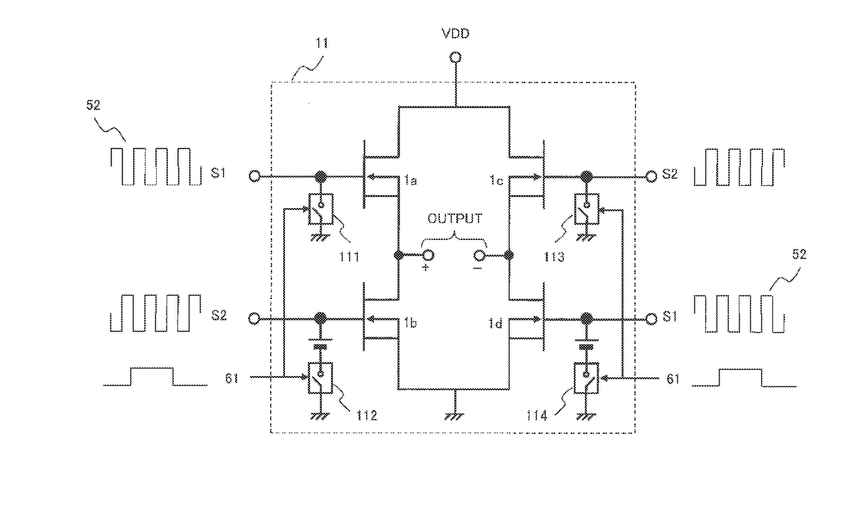
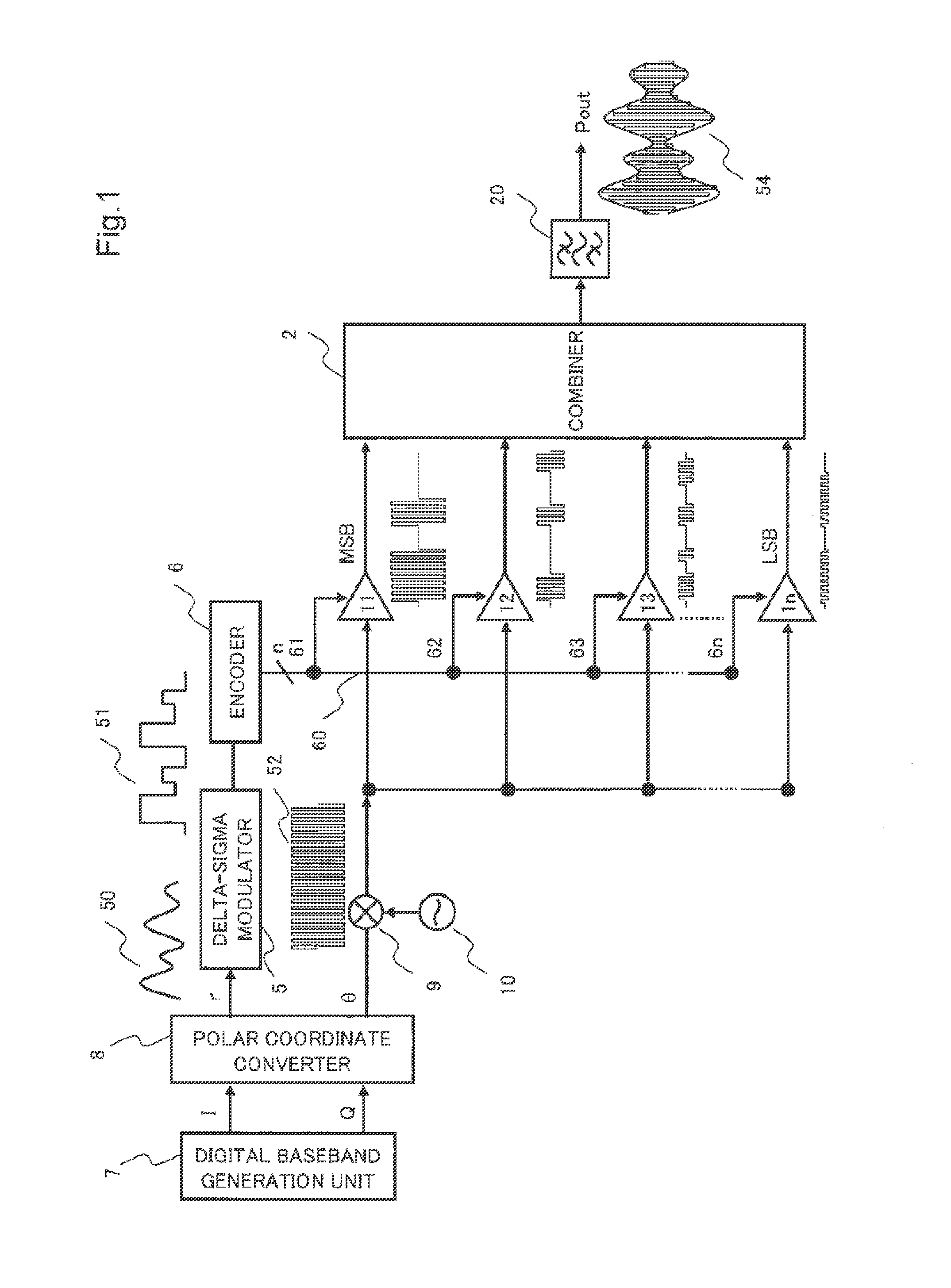
[0077]A digital baseband generation unit 7 outputs a complex signal (I, Q) of a signal to be transmitted. A polar coordinate converter 8 converts a complex signal (I, Q) into a polar coordinate signal (r, θ) and outputs. A delta-sigma modulator 5 performs multilevel delta-sigma modulation on an amplitude signal r 50, and outputs a pulse signal 51 having a plurality of discrete output levels. An encoder 6 converts the discrete output levels of the pulse signal 51 into the control signal 60 which is a digital signal of n bits and outputs. An MSB which is a most significant bit is inputted as a control signal 61, the next bit is inputted as a control signal 62, the further next bit is inputted as a control signal 63, and an LSB (Least Significant Bit) which is a least si...

second exemplary embodiment

The Second Exemplary Embodiment

Configuration

[0110]Next, a configuration of a receiving apparatus of a second exemplary embodiment is described.

[0111]FIG. 5 is a block diagram showing a configuration of a second exemplary embodiment of the present invention.

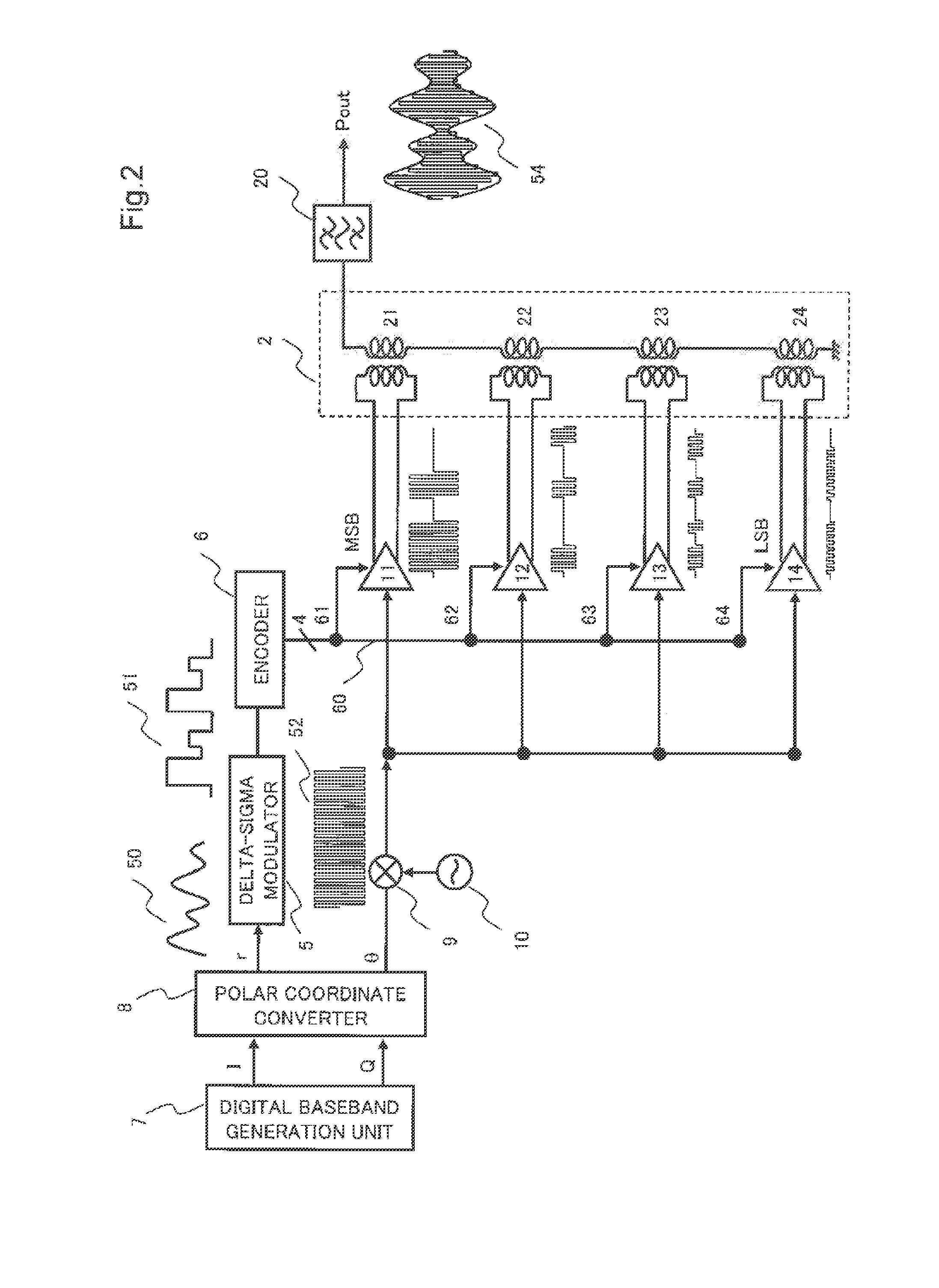
[0112]A digital baseband generation unit 7 outputs a complex signal (I, Q) of a signal to be transmitted. A polar coordinate converter 8 converts a complex signal (I, Q) into a polar coordinate signal (r, θ) and outputs. A delta-sigma modulator 5 performs multilevel delta sigma modulation on an amplitude signal r 50, and outputs a pulse signal 51 having a plurality of discrete output levels. An encoder 6 converts the plurality of output levels of the pulse signal 51 into the control signal 60 which is a digital signal of n bits and outputs. An MSB which is a most significant bit is inputted as a control signal 61, the next bit is inputted as a control signal 62, the further next bit is inputted as a control signal 63, and an LSB (...

third exemplary embodiment

The Third Exemplary Embodiment

Configuration

[0150]Next, a configuration of a receiving apparatus of a third exemplary embodiment will be described.

[0151]FIG. 7 is a block diagram showing a configuration of a third exemplary embodiment of the present invention.

[0152]Although the case where the number of power amplifiers is four is shown in the second exemplary embodiment, the number of power amplifiers is reduced to two in this third exemplary embodiment.

[0153]A digital baseband generation unit 7 outputs a complex signal (I, Q) of a signal to be transmitted. A polar coordinate converter 8 converts a complex signal (I, Q) into a polar coordinate signal (r, θ) and outputs. A delta-sigma modulator 5 performs multilevel delta sigma modulation on an amplitude signal r 50, and outputs a pulse signal 51 having discrete output levels of three valued. An encoder 6 converts discrete output levels of three valued of the pulse signal 51 into a control signal 60 which is a digital signal of 2 bits...


PUM


Abstract

An object of the present invention is to provide a power amplification device having high power efficiency for an input signal even in a power region in a large back-off.
A power amplification device of the present invention includes a delta-sigma modulator which performs a multilevel delta sigma modulation on amplitude signals of input signals, a plurality of power amplifiers which amplify carrier signals, an encoder which generates a first control signal that controls ON/OFF of the outputs from said plurality of power amplifiers in accordance with the output from said delta-sigma modulator, and a combiner which combines at least two power output from said plurality of power amplifiers in accordance with said first control signal.

Description

TECHNICAL FIELD[0001]The present invention relates to a power amplification device which is mainly used for a transmitter of wireless communication.BACKGROUND ART[0002]As a digital modulation system used for wireless communication in recent years such as a cellular phone and a wireless LAN (Local Area Network), modulation scheme such as QPSK and multilevel QAM are employed. QPSK is an abbreviation of Quadrature Phase Shift Keying, and QAM is an abbreviation of Quadrature Amplitude Modulation.[0003]In these modulation schemes, generally, signals locus forms amplitude modulation when symbol transitions occur. Accordingly, the amplitude (envelope) of a modulation signal superimposed on a carrier signal of a microwave bandwidth varies over time. The ratio of the peak power to the average power of the modulation signal is referred to as PAPR (Peak-to-Average Power Ratio).[0004]When a signal having a large PAPR is amplified, a power supply device needs to supply sufficiently large power t...

Claims


Application Information

Patent Timeline
IPC IPC(8): H03F3/217
CPCH03F3/2171H03F1/0277H03F3/211H03F3/72H03F2200/204H03F2200/336H03F2200/537H03F2200/541H03F2203/21106H03F2203/21136H03F2203/21142H03F2203/7215H03F2203/7236
Inventor KUNIHIRO, KAZUAKI
Owner NEC CORP
Why Eureka
Try Eureka