Interdigitated back contact heterojunction photovoltaic device

a back contact and heterojunction technology, applied in the direction of semiconductor/solid-state device manufacturing, semiconductor devices, electrical devices, etc., can solve the problems of reducing the short circuit current of the solar cell accordingly, affecting the photogeneration of carriers in these materials, and affecting the absorption loss

Inactive Publication Date: 2014-08-14
IBM CORP
View PDF2 Cites 28 Cited by
  • Summary
  • Abstract
  • Description
  • Claims
  • Application Information

AI Technical Summary

Benefits of technology

[0008]Another photovoltaic device includes a Si-containing crystalline substrate having a first dopant conductivity and an interdigitated back contact having back surface field stacks and emitter stacks. A front surface field structure includes a hydrogenated Si-containing crystalline layer formed on the substrate and a hydr

Problems solved by technology

In such cases, the presence of the intrinsic and/or doped a-Si:H containing material at the front surface results in some absorption loss reducing the short circuit current of the solar cell accordingly.
Due to the presence of a large density o

Method used


Image

  • Interdigitated back contact heterojunction photovoltaic device
  • Interdigitated back contact heterojunction photovoltaic device
  • Interdigitated back contact heterojunction photovoltaic device

Examples


Embodiment Construction

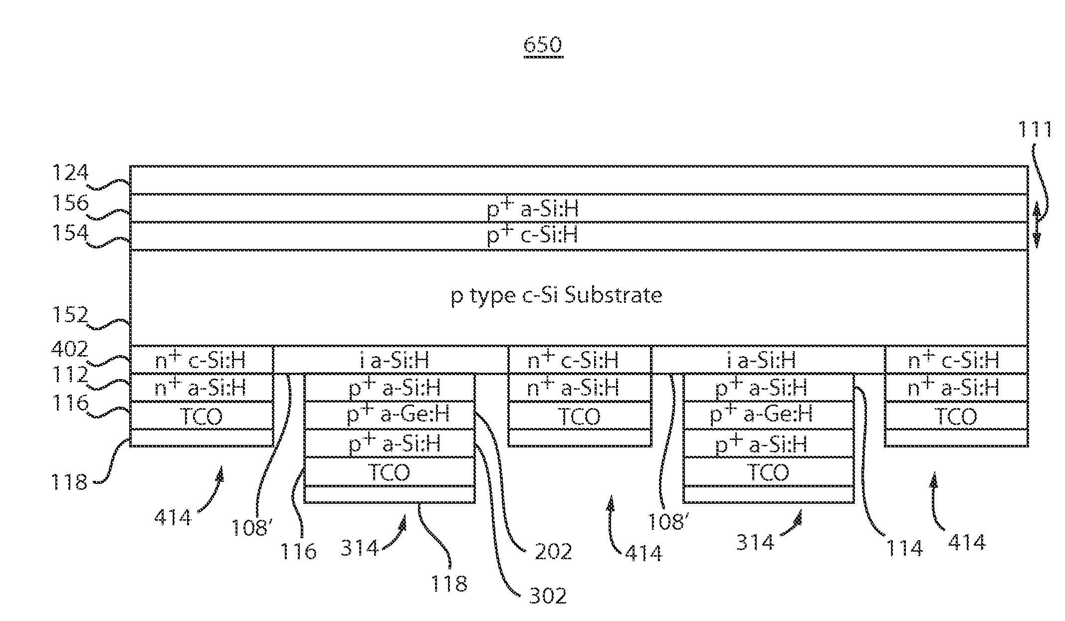
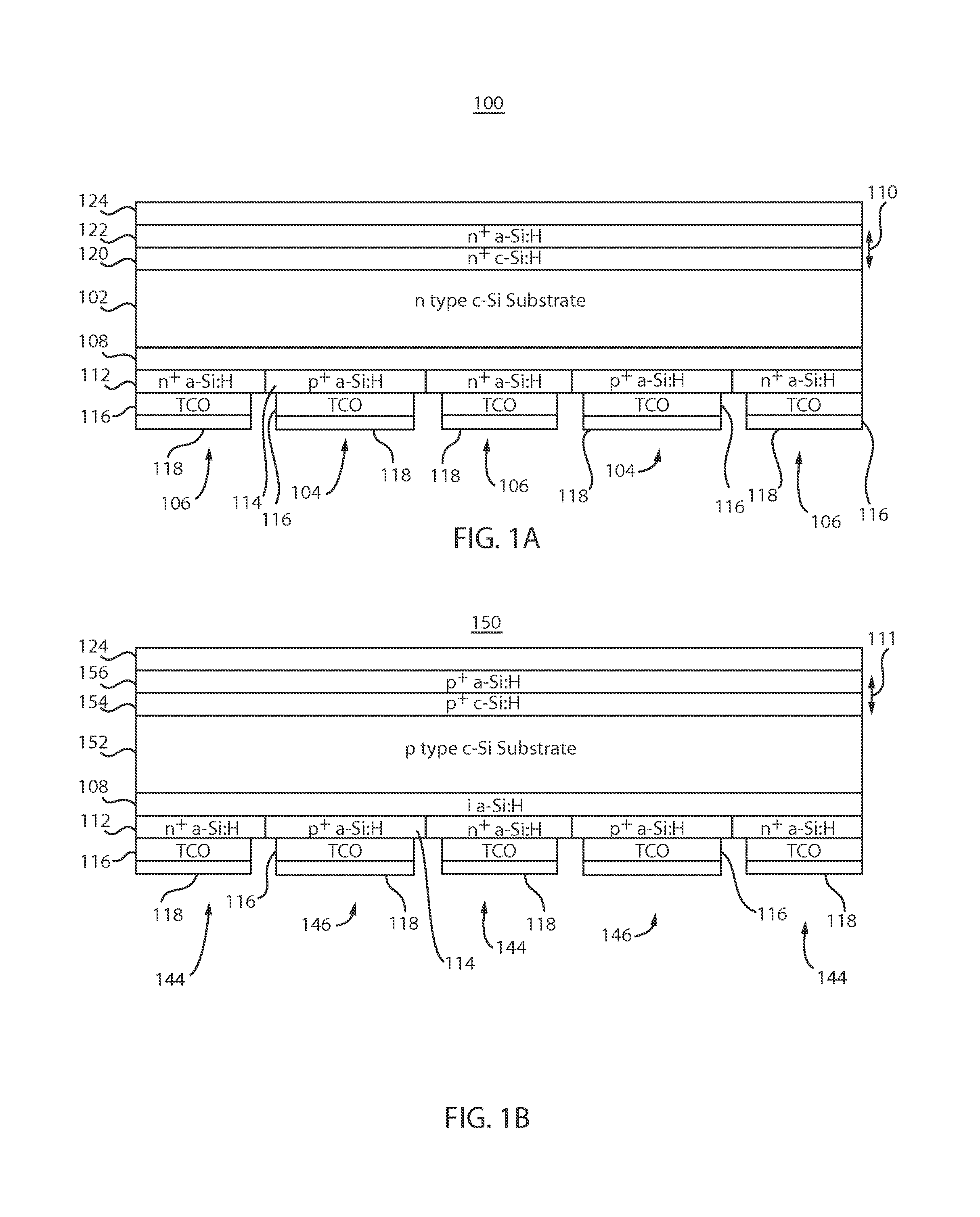
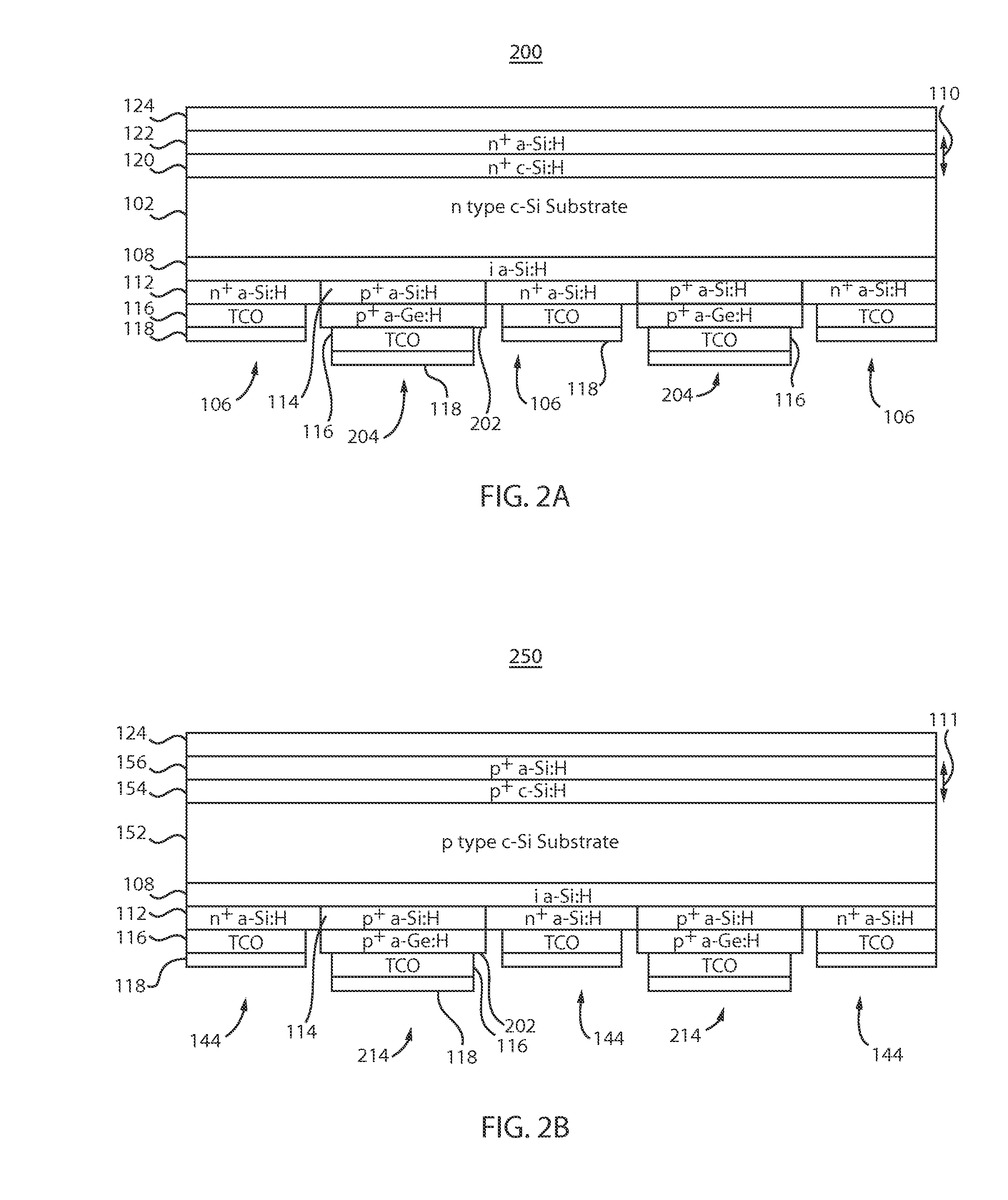
[0026]In accordance with the present principles, inter-digitated back-contact photovoltaic devices and methods for fabrication are provided. The photovoltaic devices include a front surface field (FSF) junction having a crystalline layer and a noncrystalline layer formed on a crystalline substrate. The crystalline layer, noncrystalline layer and substrate have a same dopant conductivity. In one embodiment, the crystalline layer includes hydrogenated crystalline Si (c-Si:H) having the same conductivity type as that of the substrate. The substrate may include c-Si, and the noncrystalline layer may include a hydrogenated non-crystalline material, which is either intrinsic or has the same conductivity type as that of the crystalline layer (doped c-Si:H) and the substrate (c-Si).

[0027]In one embodiment, the crystalline layer is thinner than a diffusion length of minority carriers in the crystalline layer, and has a higher doping than that of the substrate. The crystalline layer may be hy...


PUM


Abstract

A photovoltaic device includes a crystalline substrate having a first dopant conductivity, an interdigitated back contact and a front surface field structure. The front surface field structure includes a crystalline layer formed on the substrate and a noncrystalline layer formed on the crystalline layer. The crystalline layer and the noncrystalline layer are doped with dopants having a same dopant conductivity as the substrate. Methods are also disclosed.

Description

RELATED APPLICATION DATA[0001]This application is related to commonly assigned application serial no. (TBD) (Attorney Docket Number YOR920120956US1 (163-601)), entitled: “INTERDIGITATED BACK CONTACT HETEROJUNCTION PHOTOVOLTAIC DEVICE WITH A FLOATING JUNCTION FRONT SURFACE FIELD”, filed concurrently herewith and incorporated herein by reference.BACKGROUND[0002]1. Technical Field[0003]The present invention relates to photovoltaic devices and fabrication methods, and more particularly to a front surface field junction for interdigitated back contact devices.[0004]2. Description of the Related Art[0005]Inter-digitated back-contact (IBC) solar cell structures are of interest for increasing short circuit current (Jsc) (and therefore efficiency) of the solar cells by forming both an emitter junction, a back surface field (BSF) junction and the associated metallization on a backside of the solar cell. This permits sunlight to enter from a front side with minimum shadowing loss. In the case ...

Claims


Application Information

Patent Timeline
IPC IPC(8): H01L31/077H01L31/18
CPCH01L31/182H01L31/077H01L31/02167H01L31/022441H01L31/0747Y02E10/546Y02E10/547H01L31/022458H01L31/0682Y02E10/50
Inventor CHEN, TZE-CHIANGHEKMATSHOARTABARI, BAHMANSADANA, DEVENDRA K.SHAHRJERDI, DAVOOD
Owner IBM CORP
Why Eureka
Try Eureka