Organic light emitting device

a light-emitting device and organic technology, applied in thermoelectric devices, electroluminescent light sources, nano-informatics, etc., can solve the problems of degrading light-emitting characteristics, difficult to accurately control the thickness of each layer, and degrading color expression, so as to reduce the number of transistors of peripheral circuits, reduce driving voltage, and increase the aperture ratio of devices

Inactive Publication Date: 2014-08-21
IUCF HYU (IND UNIV COOP FOUNDATION HANYANG UNIV) +1
View PDF5 Cites 18 Cited by
  • Summary
  • Abstract
  • Description
  • Claims
  • Application Information

AI Technical Summary

Benefits of technology

[0021]According to embodiments of the present invention, since an organic light emitting device achieves its own active operation by employing a transistor structure, the number of transistors of a peripheral circuit can be reduced. Accordingly, there is an effect in that an aperture ratio of a device is increased and a driving voltage is decreased.
[0022]In addition, it is easy to ensure current stability during device operation by controlling charges injected into a light emitting layer using a voltage of a control electrode. Further, by adopting a light-color changing insulating layer which performs roles of insulation and light color change, attenuation of external quantum efficiency is low, and the cost of manufacturing process can be reduced.
[0023]However, the technical effects of the present invention are not limited to the above disclosure; other technical effects may become apparent to those of ordinary skill in the art based on the following descriptions.

Problems solved by technology

However, there are problems in that it is difficult to accurately control the thickness of each layer configuring the organic thin film, and light emitting characteristics are degraded due to the non-uniform thickness of the organic thin film.
There is a problem in that the reflected external light interferes with light generated from the organic light emitting device and degrades color expression.
However, since the polarizing plate cuts off portions of light generated from the inside, it degrades display efficiency.
However, the additional driver circuit reduces a light emitting area of a device, and thereby reduces an aperture ratio.

Method used


Image

  • Organic light emitting device
  • Organic light emitting device
  • Organic light emitting device

Examples


Embodiment Construction

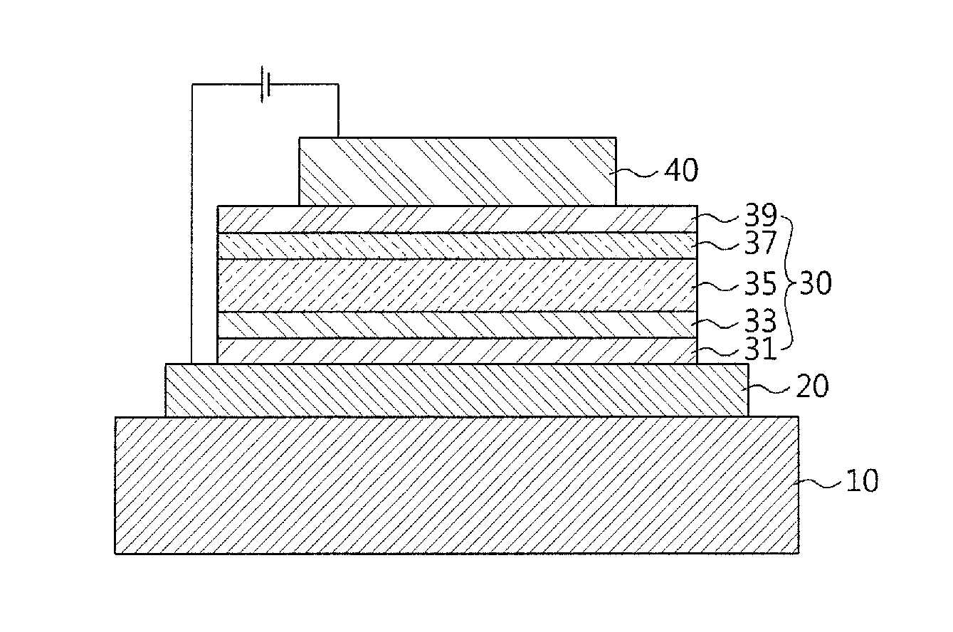
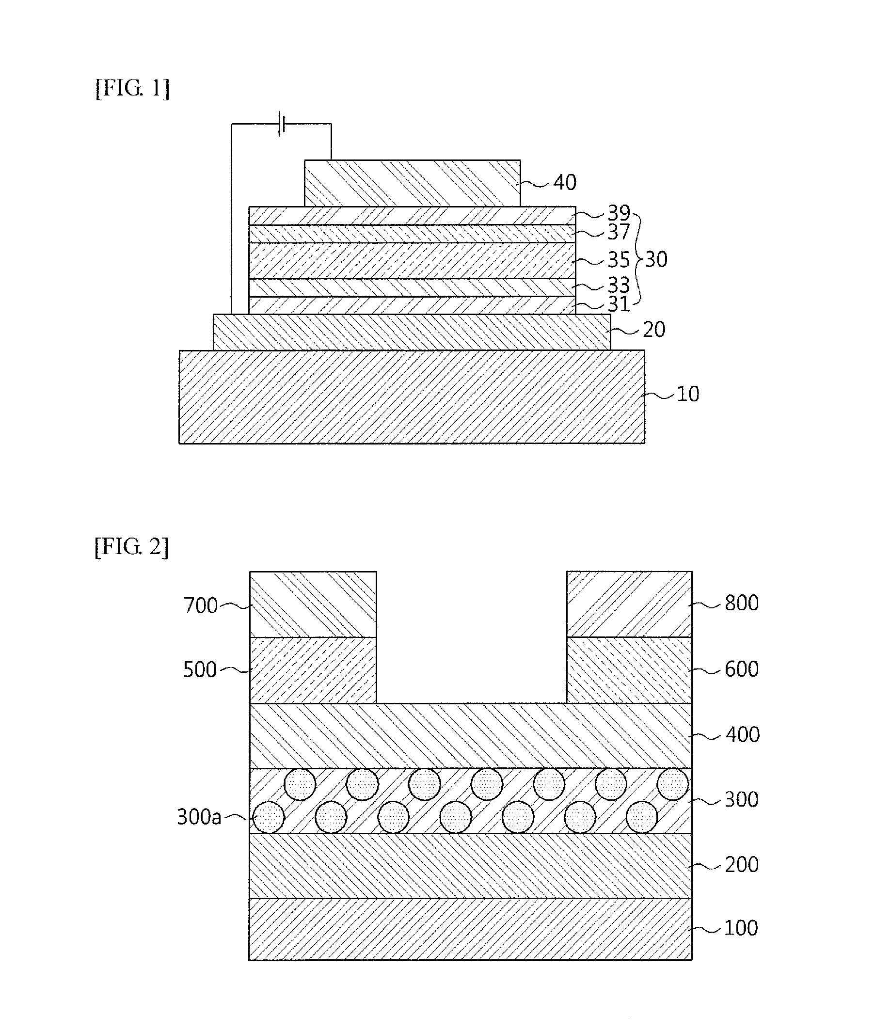
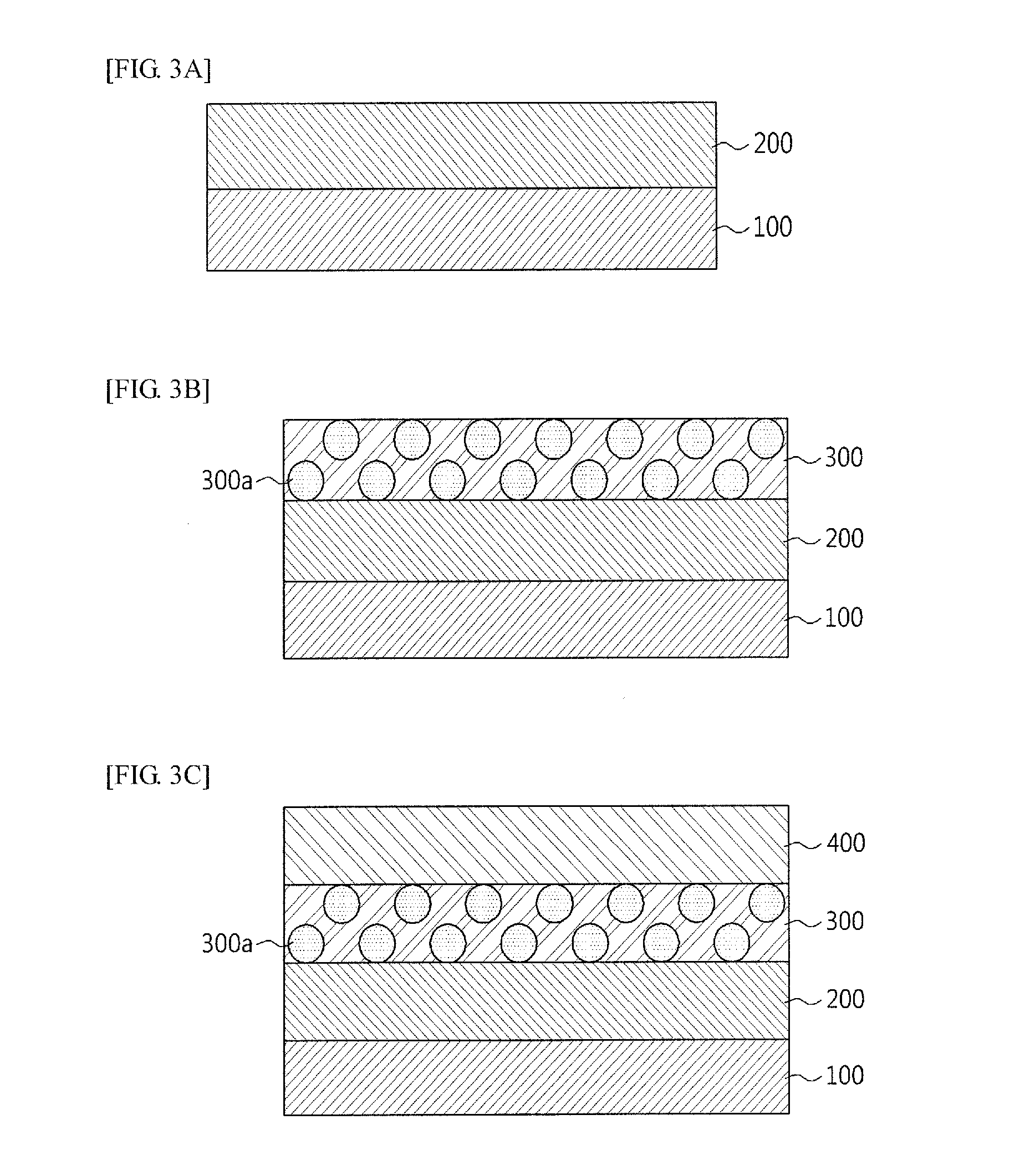
[0027]Hereinafter, embodiments of the present invention will be fully described with reference to the accompanying drawings. The present invention may, however, be embodied in different forms and should not be construed as limited to the embodiments set forth herein. The present invention should be understood to include all the equivalents and substitutions included in the spirit and scope of the present invention.

[0028]It will be understood that when a layer is referred to as being “on” another layer or a substrate, it can be directly on the other layer or substrate, or a third layer may be interposed therebetween. In addition, directional terms, such as “an upper side,”“an upper (portion),” and “an upper surface” can be understood to have meanings such as “a lower side,”“a lower (portion),” and “a lower surface” depending on their criteria. That is, spatial direction terms should be construed as relative directions, and should not be limitedly construed as absolute directions.

[002...


PUM

PropertyMeasurementUnit
diameteraaaaaaaaaa
coloraaaaaaaaaa
fluorescentaaaaaaaaaa

Abstract

Provided is an organic light emitting device including a nano composite layer. The organic light emitting device adopts a nano composite layer including an insulator and light emitting nano-particles within a device, thereby simultaneously insulating a control electrode and changing the color of light emitted from a light emitting layer, thereby improving external quantum efficiency. Further, the amount of electron holes and electrons injected into the light emitting layer may be adjusted through a voltage applied to the control electrode so as to secure a stable current when the device is operated. In addition, when compared to a conventional light emitting device, the surface area of positive and negative electrodes may be reduced so as to reduce reflectance with respect to external light.

Description

TECHNICAL FIELD [0001]The present invention relates to a light emitting device, and more specifically, to an organic light emitting device.BACKGROUND ART [0002]In broad terms, photoelectric devices are devices that convert light energy to electric energy, or vice versa. For example, photoelectric devices include organic light emitting devices, inorganic light emitting devices, and solar cells.[0003]In particular, among photoelectric devices, organic light emitting devices (organic light emitting diodes: OLEDs) have recently been in the spotlight according to a growing demand for flat panel displays.[0004]An organic light emitting device is a device which converts electric energy to light energy by applying a current to an organic light emitting material. An organic light emitting device may have a structure in which a functional organic thin film is inserted between an anode and a cathode.[0005]FIG. 1 is a cross-sectional view schematically showing an example of an existing organic ...

Claims


Application Information

Patent Timeline
Patent Type & Authority Applications(United States)
IPC IPC(8): H01L51/52
CPCH01L51/5203H10K85/221H10K50/115H10K50/30B82Y10/00H10K59/805H05B33/22H10K50/11H10K50/805H10K50/84
Inventor KIM, TAE WHANBANG, HYUN SUNGCHOO, DONG CHUL
Owner IUCF HYU (IND UNIV COOP FOUNDATION HANYANG UNIV)
Why Eureka
Try Eureka