Display device and manufacturing method of display device

a technology of display device and manufacturing method, which is applied in the direction of semiconductor devices, instruments, optics, etc., can solve the problems of metal ions eluted to the tft layer and damage to the

Active Publication Date: 2014-08-21
JAPAN DISPLAY INC
View PDF4 Cites 8 Cited by
  • Summary
  • Abstract
  • Description
  • Claims
  • Application Information

AI Technical Summary

Benefits of technology

[0011]In the above-described display device according to the present invention, the warpage deformation which occurs when substra...

Problems solved by technology

If the chemically strengthened substrate is used as a substrate to form thin fil...

Method used


Image

  • Display device and manufacturing method of display device
  • Display device and manufacturing method of display device
  • Display device and manufacturing method of display device

Examples


first embodiment

[0039]

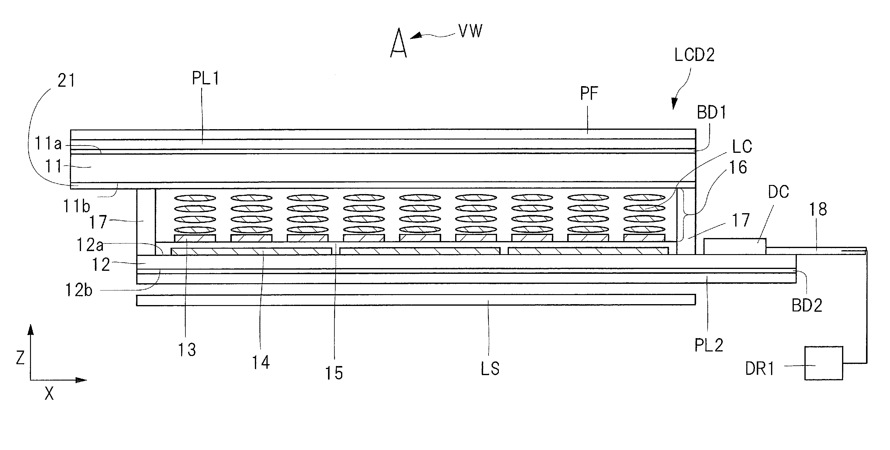
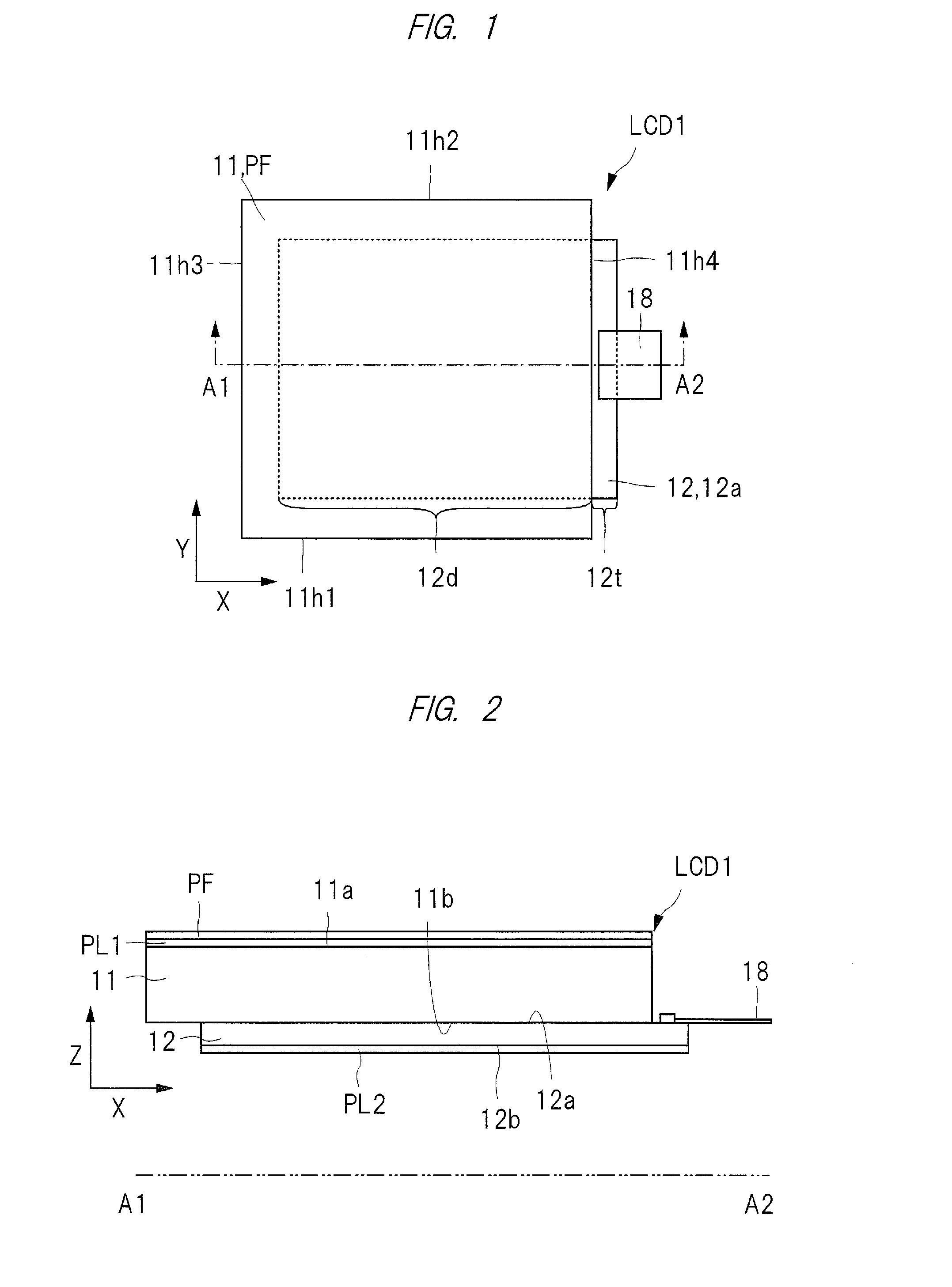
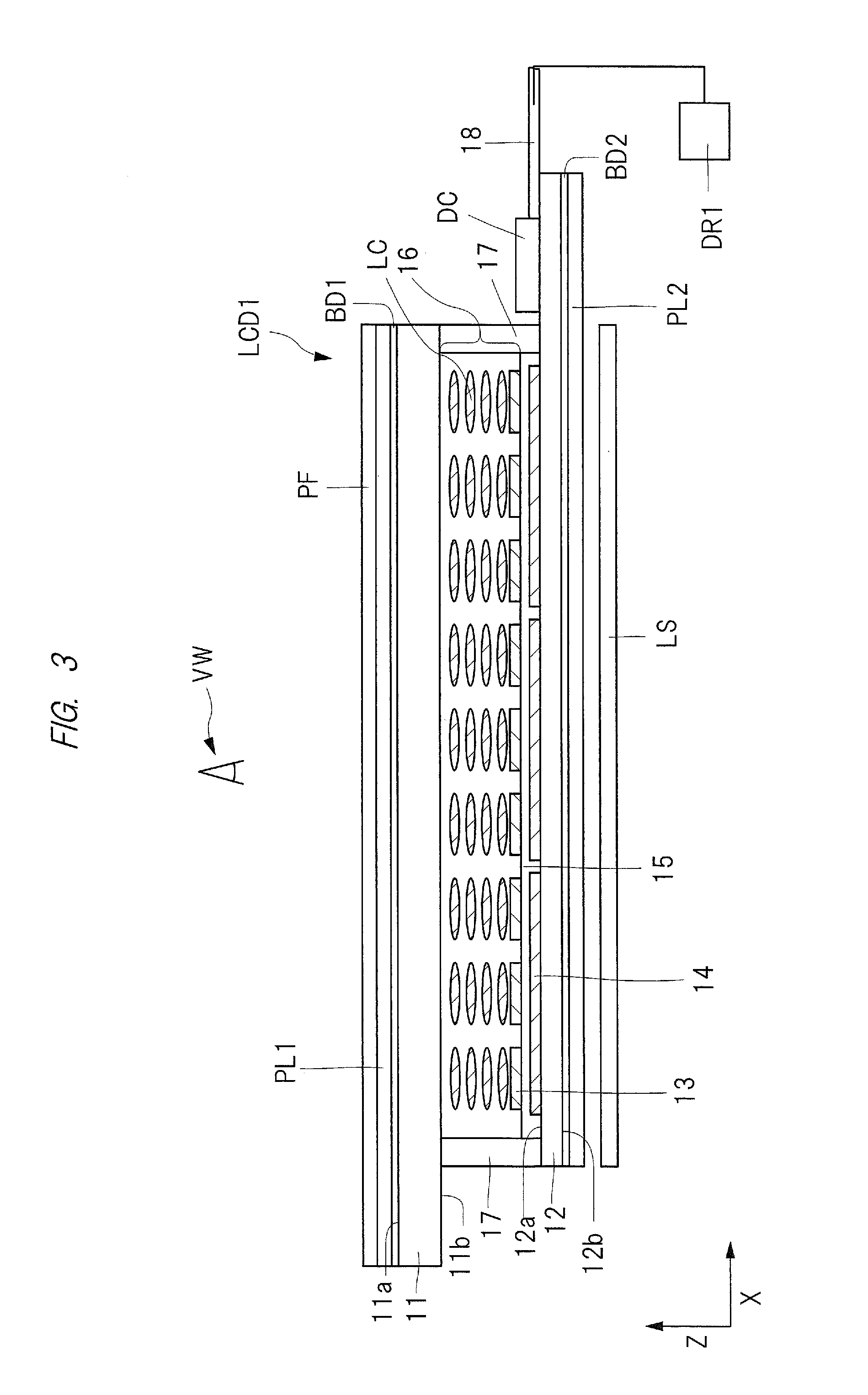
[0040]First, a basic structure of a display device will be described. FIG. 1 is a plan view showing an example of the display device of the present embodiment, and FIG. 2 is a cross-sectional view taken along a line A1-A2 of FIG. 1. Also, FIG. 3 is a cross-sectional view schematically showing the structure of a display functional layer disposed between a pair of substrates shown in FIG. 2. FIG. 4 is a perspective view schematically showing a state in which pixels formed in each of the opposed substrates shown in FIG. 3 are overlapped. FIG. 5 is a plan view showing the pixels in FIG. 4 seen from a Z direction.

[0041]The liquid crystal layer 16 serving as a display functional layer shown in FIG. 3 is extremely thin compared with a substrate 11 and a substrate 12. For example, the thickness of the substrate 11 is 0.2 mm or more to 5.0 mm or less and the thickness of the substrate 12 is 0.1 mm or more to 1.5 mm or less, while the thickness of the liquid crystal layer 16 is about 5 ...

second embodiment

[0104]In the description of the above-described first embodiment, the display device having the image display function has been taken as an example of the display device in which a pair of substrates is disposed to be opposed to each other and bonded and fixed to sandwich a display functional layer therebetween. In recent years, there is a technique in which an input device called a touch panel (also referred to as a touch sensor) is attached to the display surface side of a display device, and when a finger or the like is brought into contact with the touch panel, contact position data is detected and output. In the present embodiment, an embodiment in which the techniques described in the first embodiment are applied to a display device with an input device obtained by attaching a display device and an input device or incorporating an input device in a display device will be described. In the second embodiment, differences from the above-described first embodiment will be mainly d...

modification examples

OTHER MODIFICATION EXAMPLES

[0127]In the foregoing, the invention made by the inventors of the present application has been concretely described based on the embodiments. However, it is needless to say that the present invention is not limited to the foregoing embodiments and various modifications and alterations can be made within the scope of the present invention.

[0128]For example, in the above-described embodiments, the embodiment in which the polarization plate PL1 is covered with the protective film PF made of, for example, resin as a protective layer which protects the polarization plate PL1 from damage, stains, and others has been described. However, a glass plate can also be used as the protective layer. When the techniques described in the embodiments above are applied, the strength of the substrate 11 can be improved and the strength required for the display device can be ensured. Therefore, even when the glass plate is used as the protective layer, the thickness of the gl...


PUM


Abstract

Warpage deformation which is caused when substrates having mutually different linear expansion coefficients are bonded to sandwich a display functional layer is suppressed. A display device has a first substrate, a second substrate bonded to the first substrate so as to be opposed to the first substrate, and a liquid crystal layer serving as a display functional layer disposed between the first substrate and the second substrate. Also, a first linear expansion coefficient of the first substrate provided in the display device is larger than a second linear expansion coefficient of the second substrate, and a first thickness of the first substrate is larger than a second thickness of the second substrate.

Description

CROSS-REFERENCE TO RELATED APPLICATION[0001]The present application claims priority from Japanese Patent Application No. 2013-028772 filed on Feb. 18, 2013, the content of which is hereby incorporated by reference into this application.TECHNICAL FIELD. OF THE INVENTION[0002]The present invention relates to a display device with an input device and a manufacturing technique thereof, and in particular relates to a display device with an input device using a capacitive sensing method and a manufacturing technique thereof.BACKGROUND OF THE INVENTION[0003]There is a technique of displaying images in a display device in which a display functional layer such as a liquid crystal layer, an organic EL (Electro-Luminescence) layer, or a fluorescent layer is disposed between a pair of substrates disposed to be opposed to each other. For example, Japanese Patent Application Laid-Open Publication No. 2012-83597 (Patent Document 1) describes a liquid crystal display device using a glass substrate ...

Claims


Application Information

Patent Timeline
IPC IPC(8): G02F1/1333
CPCG02F1/13338G02F1/1333G02F1/13452G02F2201/56G02F1/133302G02F1/133368G02F1/133528G02F2202/28H01L27/1218
Inventor WATANABE, YOSHIHIROIKEDA, MASANOBUKOITO, TAKEOISHIZAKI, KOJIKURASAWA, HAYATO
Owner JAPAN DISPLAY INC
Why Eureka
Try Eureka