Light emitting device, light emitting element mounting method, and light emitting element mounter

Active Publication Date: 2014-08-28
NICHIA CORP
View PDF11 Cites 24 Cited by
  • Summary
  • Abstract
  • Description
  • Claims
  • Application Information

AI Technical Summary

Benefits of technology

[0017]In the light emitting device, because the LED chip is mounted on the substrate by using an anisotropic conductive material as the adhesive material, the mounting process can be performed at a lower temperature compared to by using solder. Therefore, high reliability of the circuit and the like can be ensured.
[0018]In the light emitting element mounting method, the light emitting element can be mounted on the sub

Problems solved by technology

However, there is the following problem with the above-mentioned conventional light emitting devices and mounters and mounting methods of light emitting elements.
Because a light emitting element is mounted on a substrate by using solder or

Method used


Image

  • Light emitting device, light emitting element mounting method, and light emitting element mounter
  • Light emitting device, light emitting element mounting method, and light emitting element mounter
  • Light emitting device, light emitting element mounting method, and light emitting element mounter

Examples


Embodiment Construction

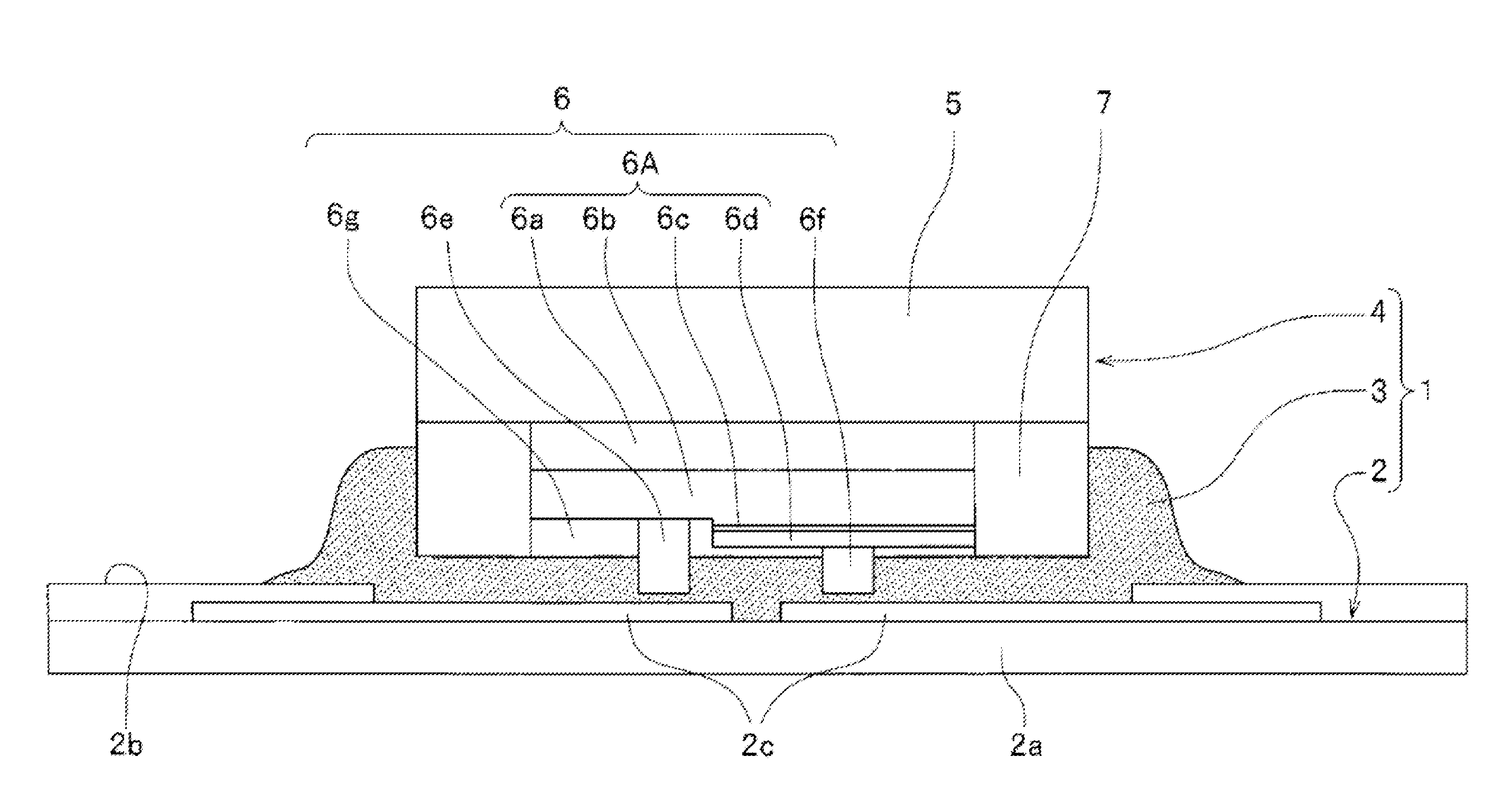
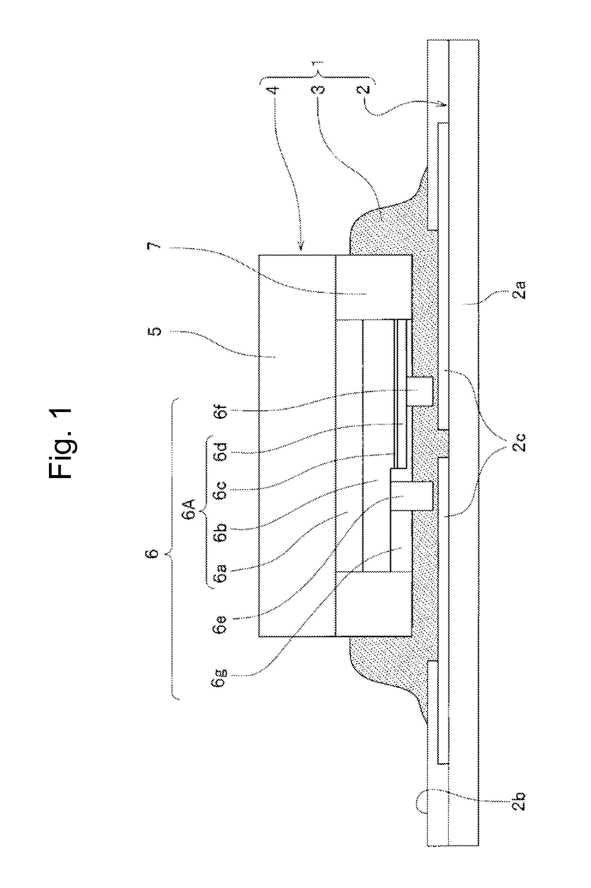
[0034]A light emitting device using a semiconductor light emitting element, a light emitting element mounting method for mounting a light emitting element of the light emitting device, and a light emitting element mounter according to embodiments of the present invention will be described below with reference to the accompanying drawings. In the following description, an exemplary configuration of the light emitting device will be firstly described, and thereafter an exemplary configuration of the light emitting mounter and an exemplary method for mounting a light emitting element will be described. The illustration of components or the like may be partly or fully exaggerated in the drawings. Furthermore, for improving readability, diagonal lines (hatching) for indicating a cross section may be omitted even in some cross sectional views.

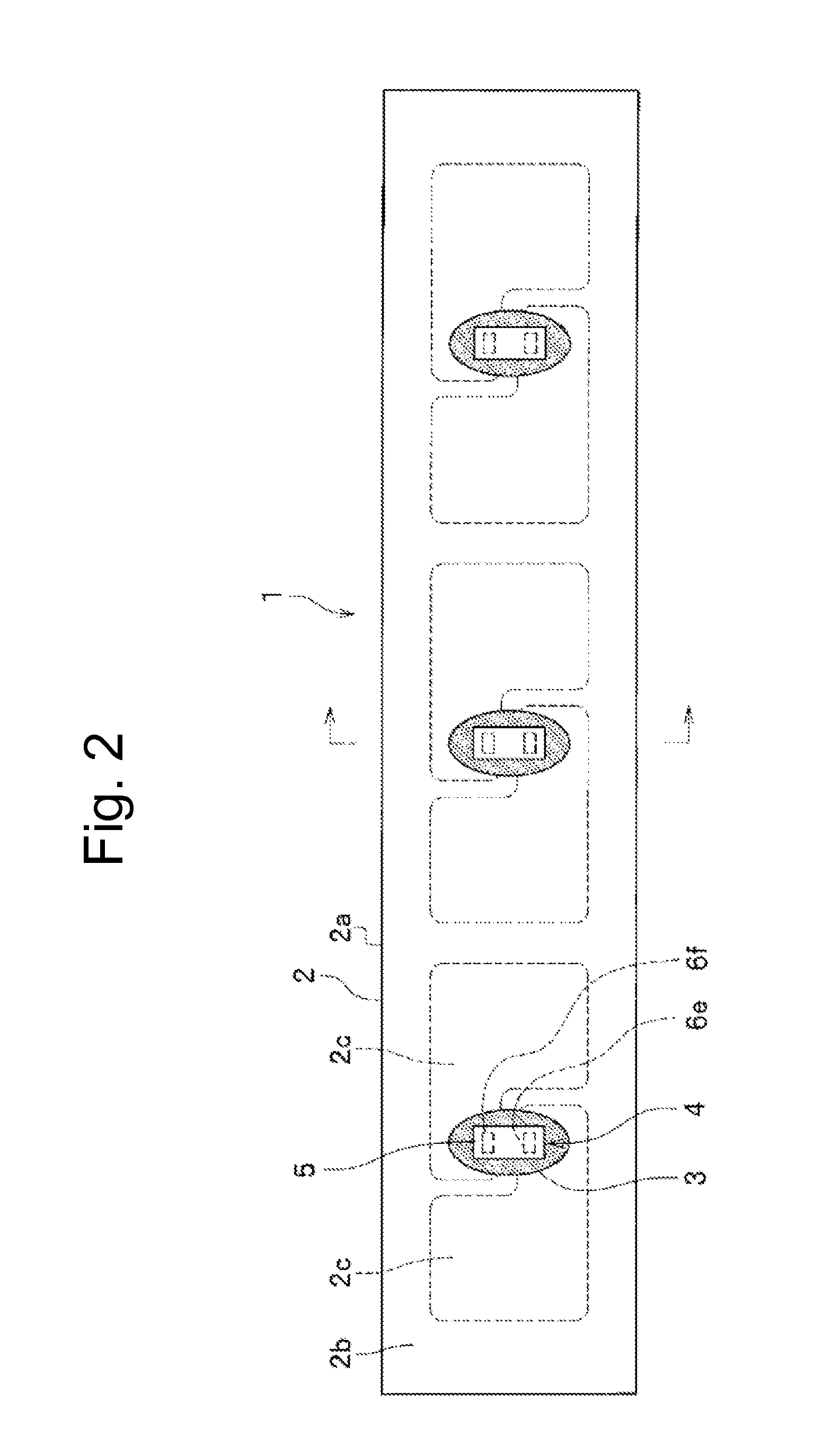
[0035]As illustrated in FIGS. 1 and 2, the light emitting device 1 of an embodiment includes a mounting substrate (substrate) 2 on which a circuit a...


PUM

PropertyMeasurementUnit
Electrical conductoraaaaaaaaaa
Anisotropyaaaaaaaaaa

Abstract

Disclosed is a light emitting device including: a light emitting element including an LED chip and a phosphor layer provided at the light emitting side of the LED chip; and a substrate on which the light emitting element is bonded by an adhesive material. The adhesive material is an anisotropic conductive material.

Description

CROSS-REFERENCE TO RELATED APPLICATIONS[0001]This application claims priority to and the benefit of Japanese Patent Application No. 2013-037982 filed Feb. 27, 2013, the entire contents of which is incorporated herein by reference.BACKGROUND OF THE INVENTION[0002]1. Field of the Invention[0003]The present invention relates to a light emitting device using a light emitting element, a light emitting element mounting method for mounting the light emitting element of the light emitting device, and a light emitting element mounter.[0004]2. Description of Related Art[0005]Typical light emitting devices using a semiconductor light emitting element include a substrate and a light emitting element mounted thereon. For mounting light emitting elements, a variety of mounting methods have been proposed. An example of such mounting methods includes a former step of applying adhesive onto an element mount area of a substrate by means of a dispenser or the like, and a latter step of bonding and mou...

Claims


Application Information

Patent Timeline
IPC IPC(8): H05K3/30H01L33/50
CPCH05K3/305H01L33/50H01L24/75H01L33/46H01L33/505H01L33/62H01L2224/73204H01L2224/83192H01L2933/0066H05K3/321H05K13/046H05K13/0469H05K2201/10106H05K2203/0195Y10T29/4913Y10T29/53178
Inventor OYU, TAKAHIROMIYATA, TADAAKI
Owner NICHIA CORP
Why Eureka
Try Eureka