Exposure apparatus and exposure method thereof

a technology of exposure apparatus and exposure method, which is applied in the direction of photomechanical apparatus, instruments, printers, etc., can solve the problems of complex and time-consuming photolithography process of semiconductor manufacturing technology, and the yield of existing exposure apparatus may still be relatively low

Active Publication Date: 2014-09-11
SEMICON MFG INT (SHANGHAI) CORP
View PDF9 Cites 16 Cited by
  • Summary
  • Abstract
  • Description
  • Claims
  • Application Information

AI Technical Summary

Problems solved by technology

The complex and time-consuming photolithography process of the semiconductor manufacturing technology is mainly performed by corresponding exposure a

Method used


Image

  • Exposure apparatus and exposure method thereof
  • Exposure apparatus and exposure method thereof
  • Exposure apparatus and exposure method thereof

Examples


Embodiment Construction

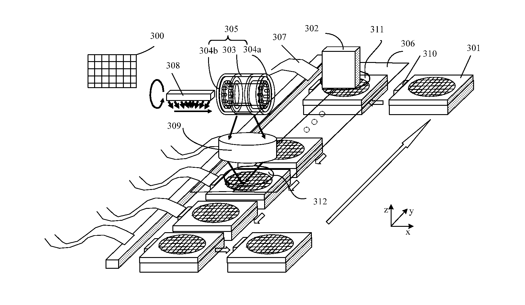
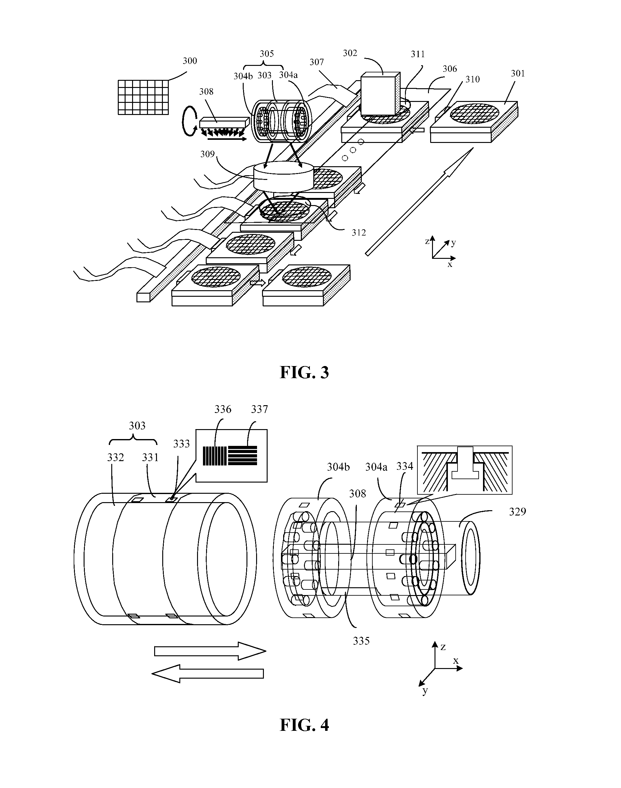
[0017]Reference will now be made in detail to exemplary embodiments of the invention, which are illustrated in the accompanying drawings. Wherever possible, the same reference numbers will be used throughout the drawings to refer to the same or like parts.

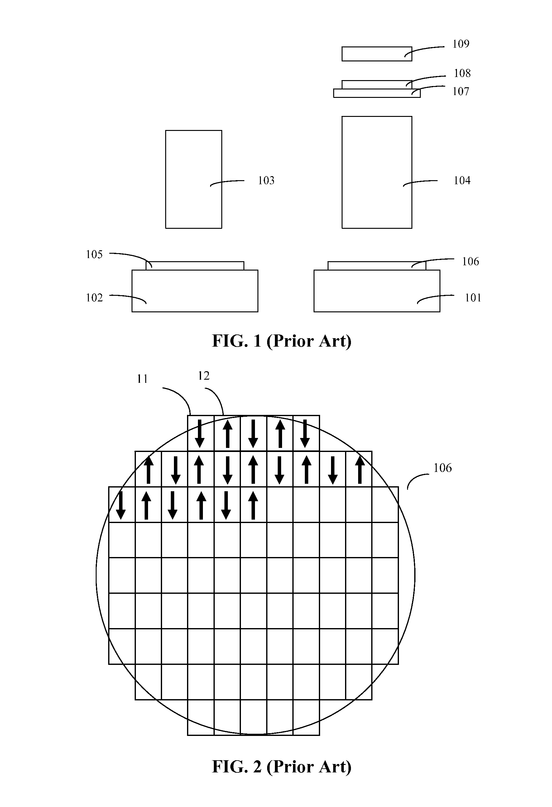
[0018]FIG. 2 illustrates scanning directions of the existing exposure apparatus for each exposure regions of a wafer, i.e., the direction of an arrow may refer to the scanning direction. For example, referring to FIG. 1, for each scanning, the stage (the first stage 101 or the second stage 102) may move along the scanning direction, and the mask stage 107 with the mask 108 may move along an opposite direction, and a first exposure region may be exposed. After exposing the first exposure region, a second exposure region may be exposed.

[0019]As shown in FIG. 2, the first wafer 106 may have a plurality of exposure regions. Referring FIGS. 1-2, the first stage 101 may move along a first direction to scan and expose a first exposure reg...


PUM


Abstract

A wafer alignment system is provided for performing a unidirectional scan-exposure. The wafer alignment system includes a plurality of wafer stages successively moving from a first position to a second position of a base cyclically. The wafer alignment method also includes an encoder plate having a first opening and a second opening. Further, the wafer alignment system includes a plurality of encoder plate readers and a plurality of wafer stage fiducials on the wafer stages. Further, the wafer alignment system also includes an alignment detection unit above the first opening of the encoder plate.

Description

CROSS-REFERENCES TO RELATED APPLICATIONS[0001]This application claims the priority of Chinese patent application No. 201310069924.2, filed on Mar. 5, 2013, the entirety of which is incorporated herein by reference.FIELD OF THE INVENTION[0002]The present invention generally relates to the field of semiconductor manufacturing technology and, more particularly, relates to exposure apparatus and exposure methods thereof.BACKGROUND[0003]Photolithography process is a very important process of the semiconductor manufacturing technology, which transfers patterns on a mask to a substrate by an exposure process. The photolithography process is a core step of the manufacturing of large scale integrations (LSIs). The complex and time-consuming photolithography process of the semiconductor manufacturing technology is mainly performed by corresponding exposure apparatus. Further, the development of the photolithography technology or the improvement of the exposure apparatus are mainly focused on ...

Claims


Application Information

Patent Timeline
IPC IPC(8): G03F7/20
CPCG03F7/70141G03F7/703G03F7/70725G03F7/70733G03F7/70775G03F9/7003G03F9/7088G03F1/42G03F7/24G01D5/34746H01L21/681H01L21/682
Inventor LIU, CHANGWU, QIANG
Owner SEMICON MFG INT (SHANGHAI) CORP
Why Eureka
Try Eureka